Soldering Verification of EEE parts SMD and PCBs
- Posted by Mari Carmen López
- On May 16, 2019
- 0
Soldering Verification Of Surface Mounted Devices And Printed Board Assemblies
High reliability assembled PCB prototypes as well as novel surface mounted devices (SMD) and mixed systems must be assessed according to well-defined qualification test plans. Such high-reliability verification programs are not limited to just evaluate the robustness, reliability, and performance of the product but they also address the verification of tools, fabrication procedures and involved materials, as well as the confirmation of product integrity. For instance, “European Cooperation for Space Standardization” (ECSS) standards used in space programs
- ECSS-Q-ST 70-38C “High-reliability soldering for surface mount and mixed technology”
- ECSS-Q-ST 70-08C “Manual soldering of high-reliability electrical connections”
state the requirements and procedures for the soldering verification of surface mounted and mixed technology, including the process validation for manual soldering. Similarly, the industrial standards IPC-9701 and IPC-A-610 indicate how to conduct the quality verification of soldering systems. These standards assess different facets of the solder joint such as the used materials, manufacturing processes the mutual compatibility and the durability under stress. Thus, the verification program of surface mounted assemblies defined in the ECSS standards, required by European Space Agencies (ESA) projects, involves both mechanical and environmental tests (thermal cycling, vibration, and shock test) and visual inspections (external and microsection analyses). This soldering verification process ensures that SMDs, substrates, solder alloys, soldering processes, associated staking compounds and conformal coatings are suitable for the operational lifetime of the spacecraft.
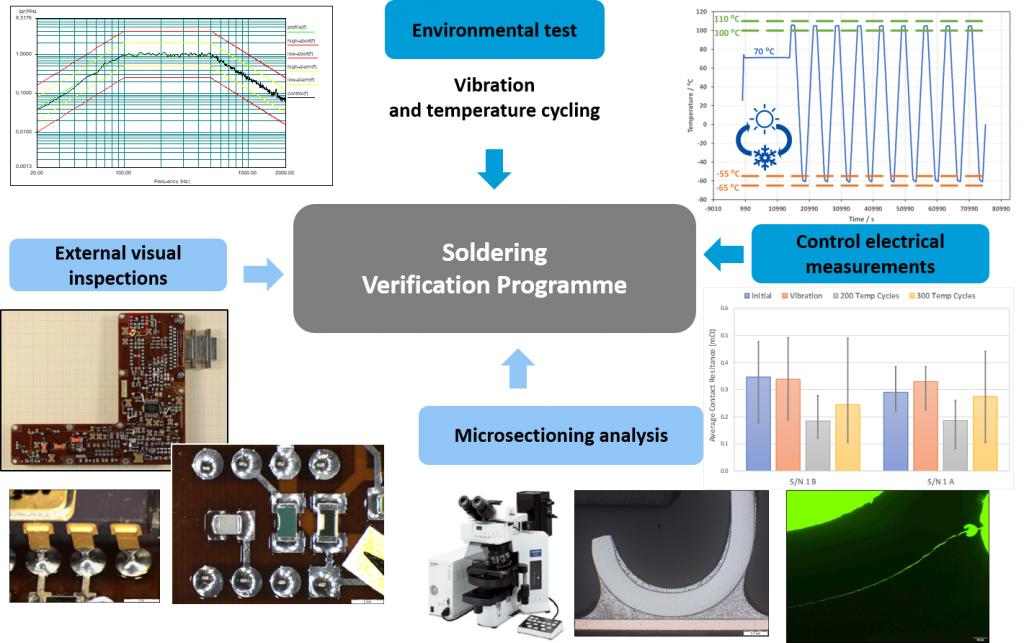
The following figure illustrates the tests involved in the ECSS soldering verification plan described in the current post. In this and other SMD verification programs, solder joints evaluation is typically conducted on PCB test vehicles specifically devised to explore the design, fabrication and process limits of a given technology and of commercial prototypes.
External visual inspection
Visual examination by optical microscopy is routinely used to study surface features, finishes and the soldering quality and integrity of solder joints. However, only qualified inspectors are able to proper failure detection and interpretation according to the applicable regulation. Major points of interest during the visual inspection of solder joints are as follows:
- Degree of wetting is a measure of solder joint quality. Properly wetted joints show an uninterrupted layer of soldering material that spreads along the whole contact-pad surface. This results from the good wettability of the solder compound on the contact pads and components.
- Joints Contours are also inspected as they indicate the volume of solder deposited. The contour should be concave when the amount of solder is enough, but it shall not extend beyond the device contact (see an example of excessive solder in the figure).
- Thermal damage. Excessive heating, for instance during soldering, may result in different types of failures such as lifted pads, measling and blistering, charred, burned or melted insulation or burns on base materials.
- Damages on the devices caused during handling.
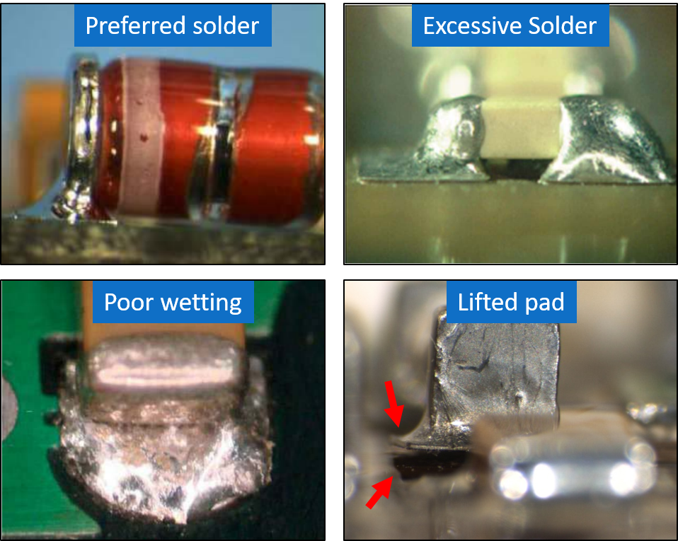
Comprehensive external visual inspection allows us to detect gross defects in solder joints. Within the ECSS-Q-ST 70-38C soldering evaluation program such optical inspection is repeated after each stress test (see examples below) in order to detect any induced anomaly.
Additionally, nondestructive inspection tools, X ray and Scanning Acoustic Microscopy, are optionally used after each stress test for the detection of hidden internal defects such as voids and solder balls under components and adhesion and delamination issues in surface mounted systems.
Vibration
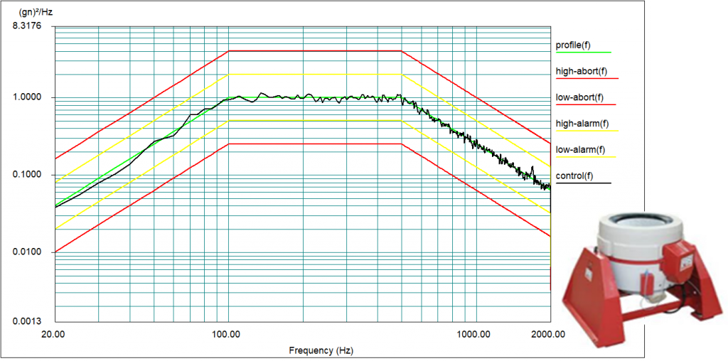
Vibration tests are performed to ascertain the ability of package and solder joints to withstand the dynamic loads related to the intended applications and environment. Vibration environment will cause stress on the PCB substrate, component packages, component leads and solder joints due to a combination of the bending moments in the PCB and the inertia of the component mass. With these concerns, the standard ECSS‐Q‐ST‐70‐08C, clause 13.2, sets out the requirements for PCB and SMD vibration testing. The severity for both random, sinusoidal and shock tests are defined depending on the application of the assembly. Thus, vibration levels for launcher hardware are more severe than those for another flight hardware.
Temperature cycling
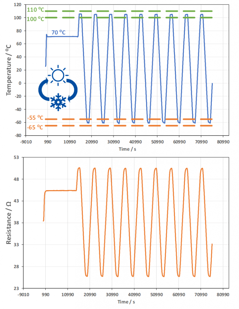
Temperature cycling is perhaps the most commonly used accelerated test. It simulates temperature-enhanced and thermomechanical stress conditions on SMD solder assemblies. Thus, the conditions of testing vary depending on the environment for which the product is designed to operate.
The standard ECSS‐Q‐ST‐70‐08C defines in clause 13.3 the requirements for this accelerated thermomechanical fatigue test that does not only involves solder-joints but also any materials interface such as PCB internal vias.
This standard imposes a large number of thermal cycles in the range of −55 °C to +100 °C, including a preliminary bake out between 60 °C and 80 °C to remove the internal humidity, which can cause unintended damages related to internal-water freezing expansion.
Continuous electrical monitoring of the daisy chain resistance (bottom figure) provides updated information about the integrity of the solder joins during this lengthy test (> 10 days) thanks to our Virtual lab platform. The assemblies are considered qualified when no degradation of the electrical continuity along the solder joint is observed during the test.

Microsectioning Analysis
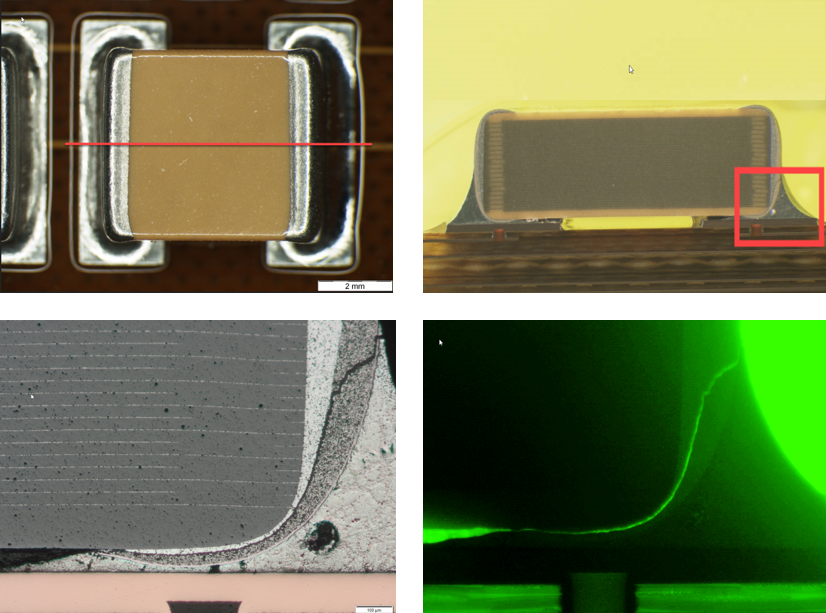
Once the PCB assembly has been submitted to environmental tests, microsectioning inspection is performed in order to evaluate carefully the PCB raw inner layers, internal solder joint integrity, and devices internal structure. Microsection analyses are mandatory for the qualification of soldering procedures in agreement to the ECSS‐Q‐ST‐70‐38C soldering verification program. This is so as it is the most reliable tool to reveal the morphology of the solder joints with respect to intermetallic formation, wetting, cracking and voiding.
Certification and compromise to quality
To fulfill the requirements of standard ECSS-Q-ST-70-38C Rev.1, this set of tests can only be carried out in a satisfactory audited ESA laboratory. Currently, Materials & Processes Laboratory of Alter Technology has been recognized as a recommended facility for such activity by the ESA authority.
Materials & Processes Laboratory team comprises highly qualified personnel (Ph.D. and Engineers) and ESA certified inspectors.

References
- Failure Modes and Mechanisms in Electronic Packages, P. Viswanadham, P. Singh, ISBN 978-1-4613-7763-4, 1998.
- Printed Circuits Handbook Sixth Edition, C.F. Coombs, ISBN 978-0-07-146734-6, 2008.
- Soldering Handbook for Printed Circuit and Surface Mounting Second Edition, H.H. Manko, ISBN 0-442-0106-3, 1995
References
Contact us
Co-Author: Francisco Javier Aparicio Rebollo
- Why Microsectioning sample preparation of PCB systems? - May 19, 2021
- Inspection of conformal coating on PCB using UV Light - August 4, 2020
- Plating Thickness Testing Overview in Alter Technology Lab. - July 28, 2020

0 comments on Soldering Verification of EEE parts SMD and PCBs