MacroVoids in assembled BGA packages
- Posted by Mari Carmen López
- On August 14, 2019
- 0
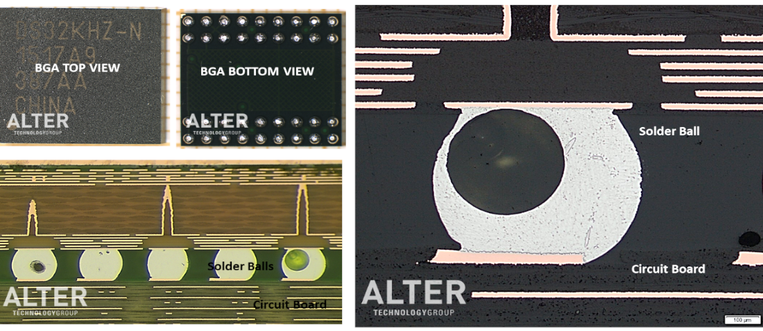
Ball Grids Array (BGA) device is metallographic prepared in ALTER TECHNOLOGY Materials & Processes Laboratory, recognized as a recommended facility for such activity by ESA authority (MEMO ESA-TECMSP-MO-013165).
Sample & Method
BGA device assembled to a PCB has been submitted to the ECSS verification programme following the guideline defined in the ECSS standard ECSS-Q-ST-70-38C. Metallographic analysis allows us to check the status of such devices after performing the environmental tests (Vibration & Thermal Cycling).
Remark of Microsectioning Inspection
An in-depth cross-section analysis allows us to evaluate the impact of voiding on the solder joint integrity of BGAs.
This microsection evaluation reveals macrovoids, also called process voids, on the solder joint. This cavity is the result of outgassing flux that has insufficient time to scape during the reflow process and it is trapped. These voids are characterized by a diameter size between 100 to 300 µm.
Contact us
- Why Microsectioning sample preparation of PCB systems? - May 19, 2021
- Inspection of conformal coating on PCB using UV Light - August 4, 2020
- Plating Thickness Testing Overview in Alter Technology Lab. - July 28, 2020


0 comments on MacroVoids in assembled BGA packages