XPS, how it works and its applications in EEE parts
- Posted by Francisco Javier Aparicio Rebollo
- On May 30, 2019
- 0
X-ray photoemission spectroscopy (XPS) also known as electron spectroscopy for chemical analysis (ESCA) is a surface-sensitive quantitative analysis method to accurately determine the elemental composition of solid materials. The technique is the most extended tool for the chemical characterization of thin films coatings and surfaces either for industrial applications as well as for research. Amongst others, this is so due to:
- The non-destructive
- The broad analysis window that cover all the elements unless H and He.
- The high sensitivity.
- For heavy metals detection limit < 0.005 % atomic concertation (ppm in weight).
- For light organic and inorganic elements detection limit < 1 %.
- Free of matrix effects which compromise the reliability of other techniques such as EDS, XRF, and FTIR.
Save time searching the EEE components of your design in doEEEt database
Practical Applications
The figure shows a representative example of the XPS survey spectrum of a sample containing both heavy and light elements of interest for technological applications. This illustrates the suitability of the technique for the simultaneous detection of either heavy and light nucleus within the limit Z > 2. Hence, XPS is one of the most reliable approaches for the non-destructive quantification of the atomic concentration in solid coatings.
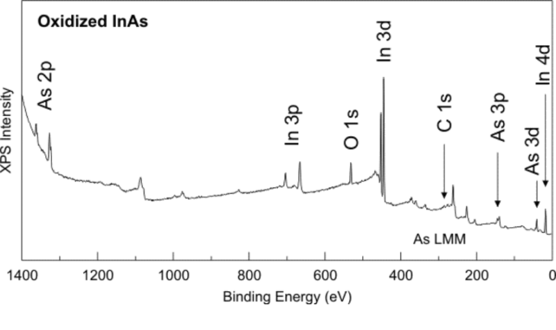
Example of XPS survey spectrum
Considering the low escape depth of the photoelectrons the inspection thickness of typical XPS instruments is of ≈ 1-3 nm. This makes this technique the most suitable for the thin-film and surface applications and processes. Nonetheless, is not so surface sensitive that the inevitable contamination developed during industrial processes completely hidden the actual sample composition, in contrast to other techniques that require ultra-high cleanliness levels only achievable by preconditioning by sputtering.
Considering the low escape depth of the photoelectrons the inspection thickness of typical XPS instruments is of ≈ 1-3 nm. This makes this technique the most suitable for the thin-film and surface applications and processes. Nonetheless, is not so surface sensitive that the inevitable contamination developed during industrial processes completely hidden the actual sample composition, in contrast to other techniques that require ultra-high cleanliness levels only achievable by preconditioning by sputtering.
XPS analysis is demanded many industrial applications where the surface composition is a critical factor:
-
- Photovoltaics.
- Electronics devices and EEE parts.
- Packaging systems.
- Display technology.
- Magnetic media.
- Corrosion (oxidation).
How it works
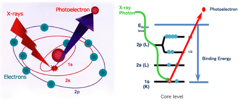
XPS working principle is based upon the photoelectric effect described in the figure.

XPS Working principle
When a photon impinges into the sample surface its energy can be absorbed completely by the electronic cloud of the atoms present in the sample. If the energy is high enough, this can cause the sample ionization and the ejection of the so-called photoelectrons with a kinetic energy that according to the Einstein equation [1] is determined by the electron binding energy of the ejected electron and photon energy.
Ekinetic = hν – Ebinding [1]
The binding energy of valence band electrons does not only depend on the elemental composition but also on the material characteristics such as the crystalline phase and others, whereas in the case of internal core electrons the binding energy is characteristics of the atoms source and the electronic level. Thus, according to this principle, XPS makes use of high energy X-ray photons to induce the photoemission of the core electrons who escape with a kinetic energy that is specific to the emitting chemical element.
Additional advantages
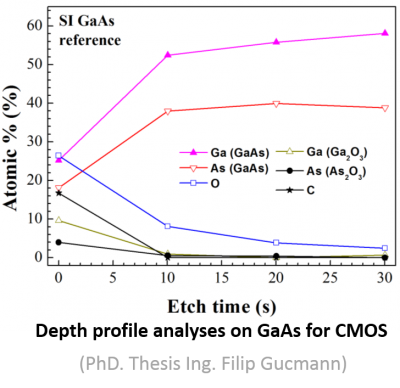
In addition to surface analyses, it is also used for the fine characterization of heterogeneous samples where the composition changes along with the depth. Thus, in combination with sputtering guns, the technique is used to perform depth profiles elemental analyses.
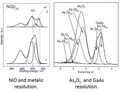
Moreover, the core energy is slightly distorted by the chemical environment what is used in an advantageous way to determine the oxidation estate of the element by fitting procedures. This is illustrated in the next figure, which shows the technique resolve the presence of metallic nickel and (Ni0) and nickel oxide (NiO) and distinguishes between arsenic oxide and gallium arsenide.
Alter Technology compromises
During the last decade, Alter technology has established a solid collaborating network with reputed research institutions and technological centers. This grant Alter access to different XPS instruments and specifically conceived for different applications: conventional XPS, depth profiles analyses. angle-resolved XPS, UPS, and others.
- Material Analysis Techniques for Electronic Components - May 6, 2022
- SAM: Survey to manufacturers and users - February 17, 2022
- What is a C-SAM Inspection? - January 29, 2022

0 comments on XPS, how it works and its applications in EEE parts