Considering the risk of retinning on QFN package
- Posted by Manuel Sánchez Ruiz
- On May 19, 2020
- 0
The use of new packages on space market has come hand in hand with the introduction of commercial of the shelf (COTS) parts in the business and even more with the New Space needs. One of those package types, widely manufactured in plastic materials, is QFN (Quad Flat No-leads) package, becoming a popular alternative to existing package types such as TSSOP.
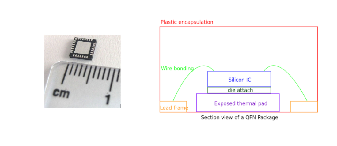
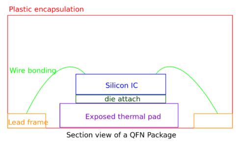
QFN packages are leadless packages where electrical connections are made through exposed lands at the bottom of the package, as well as on the perimeter, as opposed to only the connections through perimeter leads.
QFN packages allow that exposed thermal pads on the bottom of the package can connect the component to a Printed Circuit Board (PCB) by surface mounting. This connection provides a path to evacuate heat from the part die.

This kind of package provides a low manufacturing cost, small form factor and good electrical and thermal performance. This has made them to become a very popular option for new applications.
On the other hand, the increasing penetration of this package into general market implies that many manufacturers provide them in pure Sn finish to comply with RoHS directives. However, the use of pure Sn in space environment can lead to the apparition of tin whiskers, that can cause short-circuits between pins, which leaves us to implement procedures to detect pure tin at component level (as ECSS Basic Specification No. 25500 clearly details)
To avoid the risk of tin whiskers appearance, the use of pure Sn finished leads is strictly forbidden in various standard and procurement documents (as ECSS-Q-ST-60C and many quality requirements projects). The most widely technique used to avoid tin whiskers is to apply a SnPb bath to the leads (retinning). Unfortunately, due to the size and form of QFN package (lead-frame based), applying this bath can damage the package, creating alternative paths between pins or causing delamination during operation. Moreover, retinning can cause a loss of coplanarity of the leads, obstructing the correct soldering of the component.
For this reason, retinning of QFN package is considered as a risk. In different ESA projects, a Request For Deviation (RFD) has been raised by various users and approved by ESA in order to use pure Sn finished QFN packaged parts as is. The justification for this rests on various reasons:
- Pure tin is only on the bottom side of the lead, not on the lateral side of it. On the lateral side of the lead, material exposed is copper. Sometimes, central pad can be pure Sn finished too.
- As per manufacturers’ recommendations on soldering these package types, the surface of Sn termination is covered by SnPb paste during reflow (in accordance with ECSS-Q-70-38C), avoiding the exposure of pure tin.
- Some manufacturers, as for example Analog Devices, use a matte Sn finish with a post-plating treatment based of JEDEC standard JESD22A121 that allow a mitigation of tin whiskers growth.
Contact with our expert!
- Platinum Temperature Sensors Solderability Issues - May 27, 2022
- Importance of Alert and Obsolescence Management on Space Projects - February 25, 2022
- What is a PoL converter and when should I use it - November 16, 2021

0 comments on Considering the risk of retinning on QFN package