Non-Destructive Detection of Delaminations in PCBs Assemblies
- Posted by Raquel Cano Cordero
- On March 10, 2021
- 0
Summary
Sudden temperature changes (reflow soldering and temperature cycling) produce thermomechanical stress, which might generate delamination. Scanning Acoustic Microscopy is the preferred non-destructive technique for the screening of this kind of anomalies in PCB assemblies.

Development of delaminations on PCB assemblies
It is well known that one of the main sources of defects in plastic packages and COTS EEE devices is the high thermomechanical stress induced by abrupt temperature changes. Therefore, improper reflow-soldering conditions of the incompatibility with the involved materials are amongst the main factors promoting delamination and cracking within assembled plastic-encapsulated parts.
Another key fact for the development of defects in the presence of internal moisture can lead to critical failures such as “popcorn cracking”. Following IPC/JEDEC J-STD-033 (Handling, Packing, Shipping and Use of Moisture/Reflow Sensitive Surface Mount Devices), to avoid this kind of anomalies, storage and drying conditions must be selected considering the moisture-sensitive level of the component. The thermal profiles applied during the assembly process must be kept within limits set by the manufacturer. The non-destructive Scanning Acoustic Microscopy (SAM) technique ensures that the components are free of the above-described anomalies and that the mentioned precautions have been taken correctly.
Sample & Method
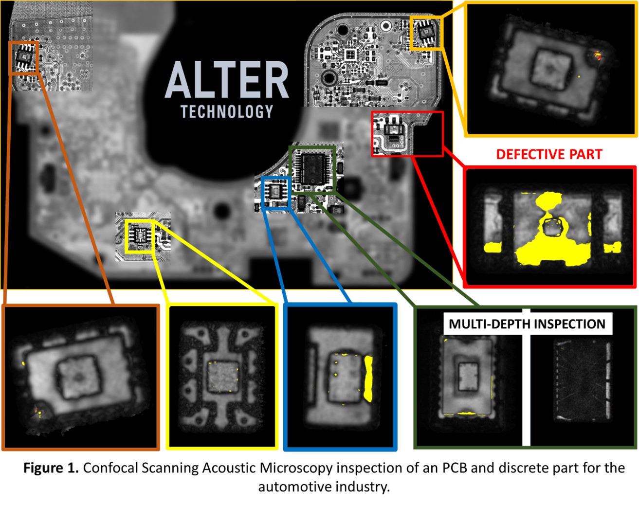
Scanning Acoustic Microscopy is performed on a Printed Circuit Board (PCB) of dimensions 15,5x10x0,5 cm. The inspection must be carried out on both sides of the PCB, as the components are mounted on both sides (a total amount of 12 different components).
The probe frequency must be adapted to the system’s characteristics, depending on what type of image we want to obtain. Thus low and high-frequency transducers with different depth of field/resolution are used. To obtain a complete image of the PCB, i.e. for a general inspection, it is necessary to work with a low-frequency transducer providing a high field depth. In contrast, the individual inspection of single components is conducted with high-frequency transducers to optimize the lateral resolution.
For PCB assemblies, both C-Mode (confocal) and A-Mode SAM inspection are compared to identify potential flaws.
Assessment
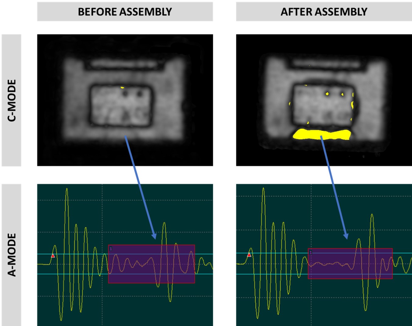
As stated above, during reflow soldering processes or thermomechanical stress (as occurred during thermal cycling), delaminations may be created. This is illustrated in Figure 2, which shows the same component before and after the PCB-assembly. In this part, delaminations have been developed during reflow soldering. The detected defect has been verified by analysing the reflected acoustic wave’s shape (A-scan inspection).

Figure 2. Confocal Scanning Acoustic Microscopy inspection of a component before and after assembly, along with the A-scanning image of the corresponding area.
GET IN TOUCH TODAY!
Do you have questions? Contact us!
- Are there Voids in your IC Plastic Molding? - November 10, 2021
- Thermo-mechanical Analyser – TMA – capabilities - October 5, 2021
- Thermo-Mechanical Analysis - August 9, 2021


0 comments on Non-Destructive Detection of Delaminations in PCBs Assemblies