ALTER has expert and reliable laboratory services in the field of engineering and testing of EEE components and equipment for space.
With cutting edge technological laboratories, and expert engineers in HI-REL, ALTER Laboratory Services include a wide range of services,…
With cutting edge technological laboratories and expert engineers in Optoelectronics and new technologies, ALTER performs optoelectronics components testing (laser, detectors, image sensors, optical transceivers, optical amplifiers, optical modulators, fibers) with specific capabilities on optoelectronics measurements as well as mechanical, thermal,…
We provide SiC testing capabilities for very extreme temperature applications, including:
– Packaging and custom assembly techniques
– Full reliability and testing capabilities include constructional, mechanical, thermal, radiation, and endurance tests, including performance validation from -190ºC to +400ºC.
ALTER SiC…
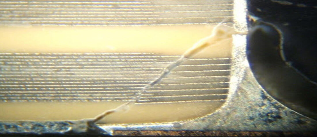
The Product/Process Change Notification (PCN) #19-001 informs about the changes in the deposition method of dielectric material, silicon dioxide, used as a protective glassivation layer over thin-film resistors
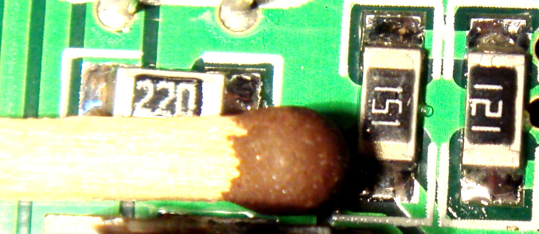
Typical short circuit failure mode in Tantalum capacitors can lead to significant damage to the adjacent circuit board, and 50%voltage de-rating alone is not sufficient to address this problem.
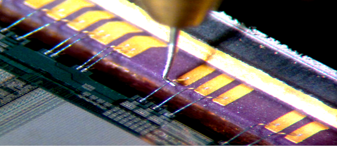
The purpose of Bond Pull Test is to measure bond strengths, to evaluate bond strength distributions and to determine compliance with specified bond strength requirements of the applicable acquisition document in order to ensure the proper manufacturing process and long-term reliability of the bonds under stress conditions, such as vibration, shock, thermal cycling or wearout phenomena.
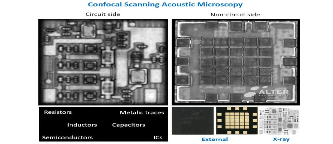
BGA device assembled to a PCB has been submitted to the ECSS verification programme following the guideline defined in the ECSS standard ECSS-Q-ST-70-38C. Metallographic analysis allows us to check the status of such devices after performing the environmental tests (Vibration & Thermal Cycling).
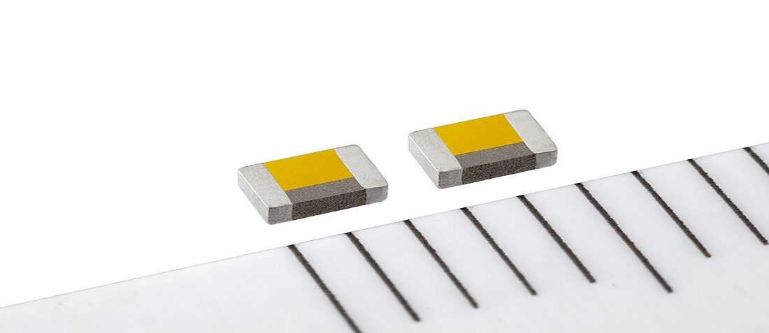
TDK Corporation (TSE:6762) announces the development of a miniaturized thin-film power inductor in an IEC 2012 case size that can handle higher currents compared to conventional products. The low-profile TFM201208ALD power inductor measures in at 2.0 x 1.25 x 0.8 mm and is available with a rated inductance of 1.0 µH.
Inside the presentation, we will cover mainly 2 topics:
1st one will consist to address packaging material, I mean Ceramic versus Organic packages,
2nd one will address relevant Quality standards with NX proposal Quality flows and pricing level versus Quantity.