Microchip’s technical experts and partners will be presenting the most innovative space-related products, capabilities, and system solutions in this one-day technology forum. The attendees will see demonstrations of how the interoperation of our latest products can accelerate their development time. They´ll also gain a comprehensive understanding of how Microchip’s Sub-QML and COTS-to-RT components help address the challenges of meeting system performance and reliability goals while also saving costs.
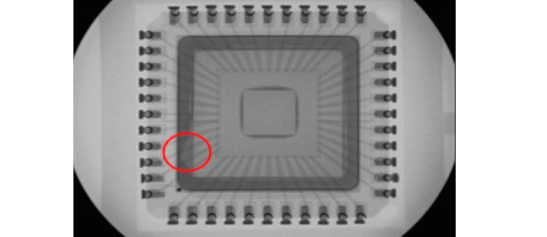
The purpose of radiographic inspection is to detect internal physical defects which are not otherwise visible in electronic components. The radiographic techniques reveal such flaws as the presence of foreign objects, improper interconnecting wires, inhomogeneities in materials, improper positioning of elements, voids in the die attach material or encapsulating, etc.
Various myths related to EEE Components are circulating due to misunderstanding and misinterpretation. The presentation attempts to debunk 16 myths, hopefully helping the community avoid pitfalls.
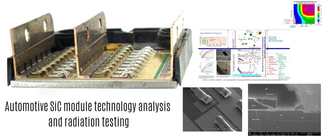
Silicon MOSFETs are also capable of handling medium levels of power and overlap in functionality somewhat. With the introduction of the 800V the need of wide band Gap technologies such as the Silicon Carbide (SiC)-based substrates are fairly new and hold even more promise with power density at higher switching frequencies and with better thermal characteristics.
Thermographic analysis techniques used in Alter Technolgy :
Infrared camera thermal maps,
Thermal behavior of equipment and cabinets,
Thermal analysis at customer specified temperature conditions.
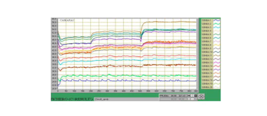
The analysis of the distribution of the dissipated heat in cabinets or enclosures gives relevant information for checking the reliability of a system and its components.
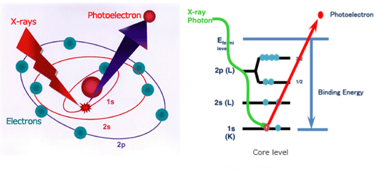
X-ray photoemission spectroscopy (XPS) also known as electron spectroscopy for chemical analysis (ESCA) is a surface-sensitive quantitative analysis method to accurately determine the elemental composition of solid materials. The technique is the most extended tool for the chemical characterization of thin films coatings and surfaces either for industrial applications as well as for research
The New Space industry resorts to this way of saving. Such a shortcut obviously is cost-efficient, but it still invokes knowledgeable, educated technical decisions. It is not enough to accept some usually undefined risks. The cost of cost-saving has to be known.
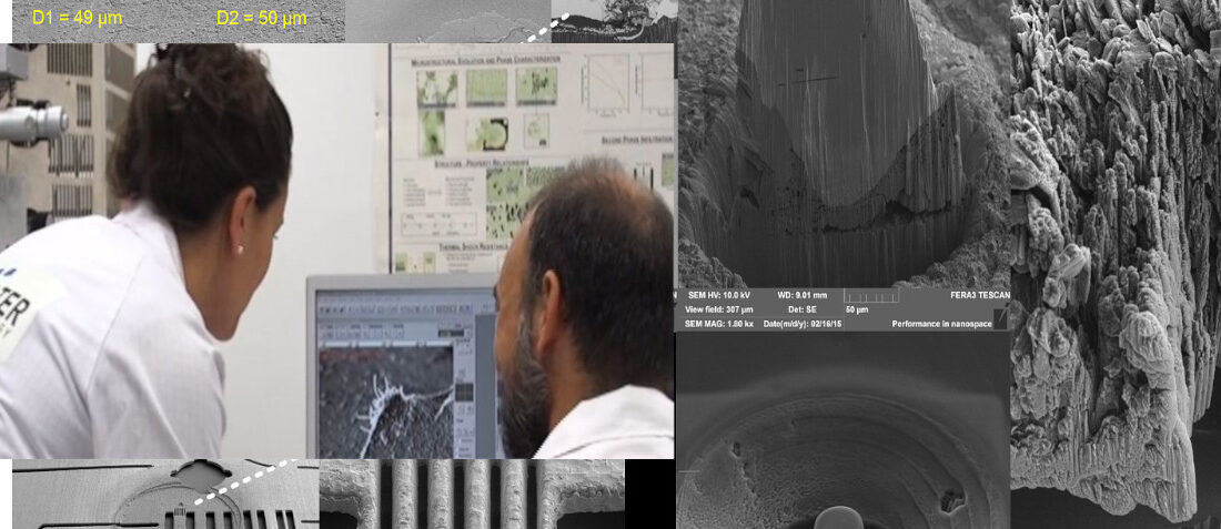
SEM available high magnification tool to analyze the design, construction or handling defects. It can be used to check the interconnect metallization on an integrated circuit: metal step coverage, etc., or for performing an in-depth technology study: reverse engineering, die cross sectioning, failure analysis, etc.
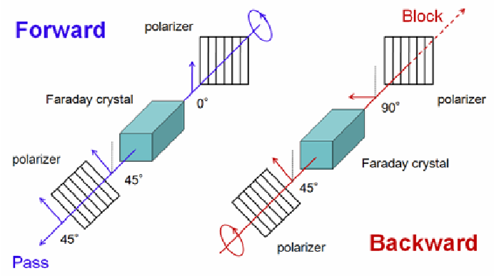
Explore the critical role of optical couplers, splitters, and isolators in space applications, where reliable communication and signal integrity are paramount. Learn how these passive components optimize bandwidth usage, enhance data transmission, and protect against reflections and noise in the challenging space environment. Discover the challenges these devices face in extreme conditions and the rigorous testing techniques, including thermal, vacuum, radiation, and mechanical characterization, ensuring their robust performance during space missions.