MEMS Packaging
- Posted by doEEEt Media Group
- On March 12, 2020
- 0
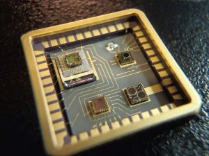
Alter Technology UK has experience in the assembly and packaging of MEMS devices.
Alter Technology UK offers customers support in prototype/process development for LED packaging and volume manufacturing capability. By prototyping on the volume manufacturing tool-set, Alter Technology UK can offer a risk-free transition to manufacturing with a fully optimized and high-yield process.
There are several specific technical challenges related to MEMS assemblies, such as special handling techniques and the restriction that many standard fluxes, adhesives, and solvents can’t be used.
As a result, Alter Technology UK has developed an extensive “tool-kit” of material and process knowledge in all key steps of the assembly process, including wafer saw, die-attach, flip-chip attach, wire bonding, and encapsulation. This Tool-Kit of process and material knowledge is used to reduce development times, reduce risk and reduce development and manufacturing risks for customers.
Advanced packaging techniques such as System-in-Package (SiP) and Wafer Scale Packaging (WSP) have also been developed to support the increasing trends in miniaturization and lower costs.
Contact us for more information
- Space-Grade components available for immediate delivery - April 10, 2025
- Exclusive stock on doEEEt: How to access and request - April 10, 2025
- Managing EEE components for LEO and lower cost space missions - December 17, 2024


0 comments on MEMS Packaging