Advantages of SAM for new space microelectronics inspection
- Posted by Javier Alejandro de la Ossa Fernández
- On March 10, 2022
- 0
SAM provides non-destructive imaging of delamination in die and package materials, widely used to new space microelectronics inspection
The global market for microelectronics is growing fast. Demand for new space microelectronics devices remains strong in the areas of defense and aerospace, automotive, power electronics, and medical technology.
This market is highly competitive, and reliable and robust non-destructive methods for quality control and failure analysis are demanded. Scanning Acoustic Microscopy (SAM) is a versatile diagnostic tool used for the semiconductor industry to investigate, measure or image microelectronic parts for detecting a long list of defects that originated during the manufacturing process due to temperature cycles, mechanical stresses as well as corrosion and electric fields.
SAM for new space microelectronics devices inspection
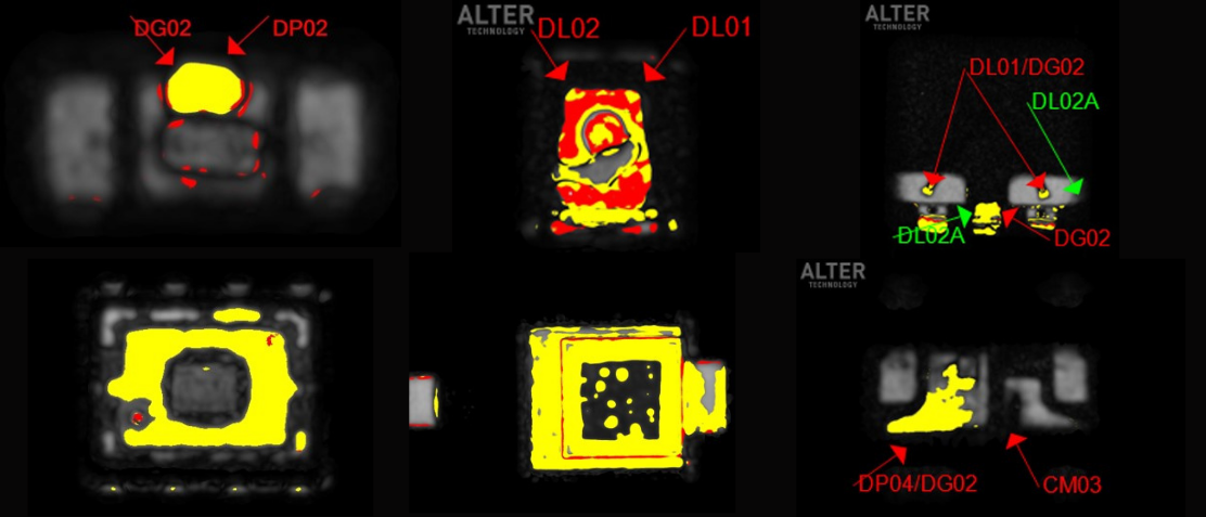
Overall, SAM is an efficient and helpful technique for imaging defects’ morphology, location, and size distribution. It can deal with the complexity of microelectronics devices where many components are gathered in a tiny volume fraction by detecting ultra-thin delamination (common defect found in plastic COTS), evaluating the risk of popcorning, or successfully seeing submicron air gaps.
Scanning Acoustic Microscopy (SAM) inspections provide the possibility of having information from different layers in materials. It is used to calculate the thickness of internal layers, interior features’ depth, and the production of three-dimensional images from defects.
There are many other methods for failure analysis in microelectronics (optical microscopy, laser decapsulation, wet etch decapsulation, SEM microscopy, TEM microscopy, X-ray, etc.). Still, the problem with most of these methods is that they are destructive. To successfully perform some of these tests, it is necessary to have a sophisticated sample preparation, which requires time and the possibility of damaging the sample during preparation.
All of it makes SAM, among others failure analysis techniques (destructive and non-destructive), one of the best and the most widely used. Despite the fact it is a complex technique and requires great skill and experience for operation and interpretation of the results.
GET IN TOUCH TODAY!
Want to contract this service? Contact us!
ALTER laboratory services: New space microelectronics inspection
In Alter Technology, the Scanning Acoustic Microscopy Lab involves a qualified (Ph.D., M.Sc.) and multidisciplinary team specialized in different disciplines such as Materials Science, Physics, Electronics; together with a highly experienced technical staff with a solid background in microscopy, materials analysis, and EEE inspection. This team is supported by more than 30 years of experience in Alter Technology in EEE testing and engineering.
The following list is a summary of the wide range of defects that can be detected in new space microelectronics inspections: die tilt, delamination between underfill (UF) and the substrate, delamination within the substrate, dielectric delamination, Lid delamination, popcorn cracks, and voids in UF, bonded wafer voids, solder cracks, etc.

Wrapping Up
SAM provides non-destructive imaging of defects and delamination in die and package materials. It is widely used to new space microelectronics inspection such as plastic encapsulated ICs, flip-chip systems, bonded wafers, printed circuit boards (PCBs), etc.
It is particularly useful for the inspection of small and complex devices. SAM is highly sensitive to defects that commonly originate under different stresses during the manufacturing process.
- Entangled photon sources for quantum communications - December 14, 2022
- Using optical transceiver technology within space vehicles - November 8, 2022
- Issue 224 of ESCC QUALIFIED PART LIST (QPL) - March 21, 2022


0 comments on Advantages of SAM for new space microelectronics inspection