Supercapacitors voltage measurements
- Posted by doEEEt Media Group
- On February 9, 2023
- 0
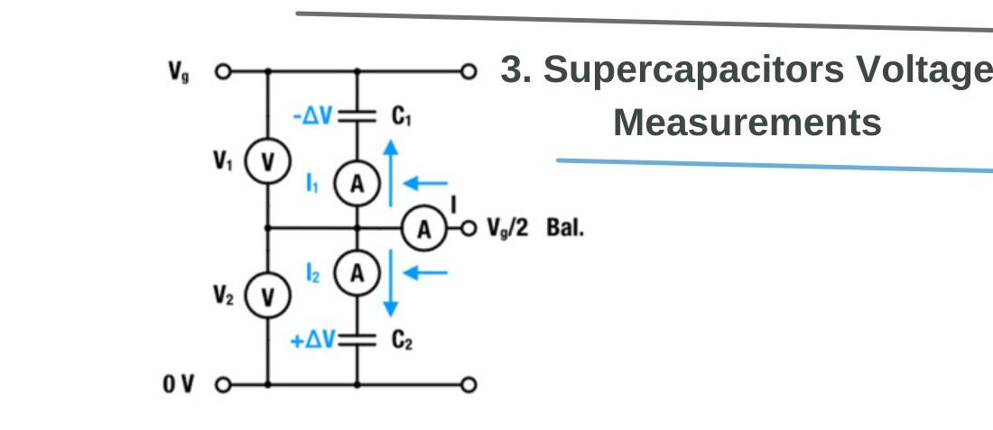
The voltage measurements were performed with a self-developed setup based on the integrated circuit CY8CKIT-059 from PSoC. The data acquisition was utilized with an Excel script. The measurement setup, including the programming of the script, was developed by Jon-Izkue Rodriguez from WE eiSos.
The power supply we used was the HMP4040 from Rohde & Schwarz. The currents for determining the power dissipation were measured with M252A METRAHit ESPECIAL Current Transformer Connection Multimeter from Gossen-Metrawatt.
We tested a series combination of two SC from WE eiSos
- Capacitor 1: C1 = 10 F
- Capacitor 2: C2 = 15 F
This practically constitutes deviations from a theoretical capacitor with a rated capacitance of Cr = 12.5F. For the charging, we used a
- charging voltage Vg = 5.4V
- max. charging current Ic = 2A
We want to underline that combining SC with different rated capacities is inadvisable for reliable circuit design. We only choose this combination for experimental purposes. This setup provides three advantages:
First, this setup provides a significant and reproducible imbalance of around ±0.5 V. We could change the set of capacitors without an intensive search for suitable mismatches. Second, it demonstrates the potential robustness of the EDLC if operated under extreme overvoltage. Although the lifetime was drastically reduced to a few weeks, none of the used SC showed a catastrophic failure. Third, it shows the operation of the individual balancing strategies under extreme conditions.
The chosen capacitors demonstrate the operation of each strategy under extreme imbalance. In practice, capacitance variation is much lower than in this example, even over different production batches. We also studied the self-discharge behavior of each circuit for a period of 24 h. Hereunto, we disconnected the entire balancing circuit from the primary power source after the capacitors were fully charged and balanced. The voltage was again measured with the PSOC CY8CKIT-059.
Based on the measurements, we also assess the circuit’s applicability in stand-alone long-term applications. In that respect, the expression “long-term” describes approximately several days.
Resistor, 1 kΩ Passive Balancing
For the passive balancing, as shown in Figure 2, we used a 0.6 W, 1kΩ (1%) resistance. We have chosen the resistance in favor of a short balancing time rather than a low power loss. The measured voltages V1 and V2 and the resulting voltage difference |V1 – V2|, given in Figure 7, show a complete balancing after around 600 min. V1 and V2 approach Vr asymptotically.
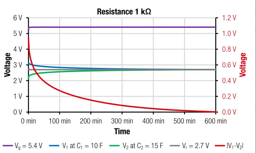
Figure 7: Time-dependent supercapacitor cell voltages V1, V2, and Vg as well as the voltage difference |V1 – V2| (corresponds to ordinate on the right-hand side) as measured for the passive balancing with resistors
The measured balancing time corresponds to the estimation given in section 4.1, tb = 625 min = 3 ∙ Rb ∙ C = 3 ∙ 1 kΩ ∙ 12.5F. The overall power dissipation (effective leakage current, Iloss) after 12h is 2.8mA ∙ 5.4V ≈ 15 mW. This balancing speed may be sufficiently fast for low-power applications or backup solutions, and the power loss is acceptable. The resistance should be increased for battery-driven (standalone) applications to reduce losses. It is advisable to reduce operating voltage to avoid overvoltage to be safe. The half-life and self-discharge time are estimated with the:
![supercapacitor half-life, self-discharge time estimation [16]](https://www.doeeet.com/content/wp-content/uploads/2023/02/supercapacitor-half-life-self-discharge-time-estimation-16.jpg)
supercapacitor half-life, self-discharge time estimation [16]
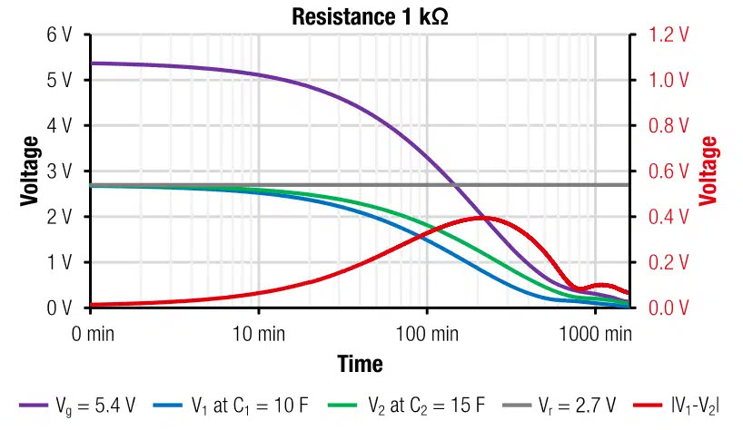
Figure 8: Measured self-discharge of supercapacitor balancing circuit with resistors. The graph shows time-dependent cell voltages V1, V2, and Vg and the voltage difference |V1 – V2| (corresponds to ordinate on the right-hand side).
The results of self-discharge measurement, as given in Figure 8, correspond to the estimated half-life self-discharge time of around 130min. The self-discharge time is large enough to consider passive balancing with 1 kΩ as suitable for a standalone solution.
Zener Diode Passive Balancing
As shown in Figure 3, we used the voltage regulator diodes BZX79-B2V7 from NXP Semiconductors for the passive balancing. The results in Figure 9 indicate a complete balancing after around 80min. With the datasheet value of total power dissipation of 500mW, the measured value fits roughly to the theoretical approximation of:

[17]
The overall power dissipation (effective leakage current, Iloss) after 12h is 5mA ∙ 5.4V ≈ 27mW. For lower voltages the power dissipation will be even lower. (The datasheet states: Iloss(1V) = 20μA).
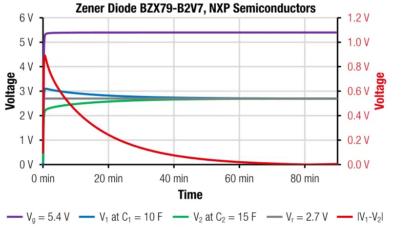
Figure 9: Time dependent supercapacitor cell voltages V1, V2 and Vg as well as the voltage difference |V1 – V2| as measured for the balancing with Zener diode BZX79-B2V7
Due to the strong nonlinear voltage dependence of Zener diodes, the calculation of the self-discharge characteristic is difficult. We may however use the same concept as for tb* and introduce a correction factor f to adjust the expression for the half-life self-discharge time. We may estimate that the data sheet value Iloss (1V) = 20μA is in our case about 10 times higher. With f = 10 the theoretical half-life self-discharge time for a stack, balanced with a Zener diode, can be estimated with:

[18]
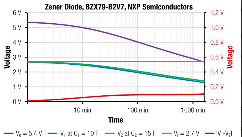
Figure 10: Measured self-discharge of supercapacitor balancing circuit with Zener diode. Graph shows time-dependent cell voltages V1, V2 and Vg and the voltage difference |V1 – V2| (corresponds to ordinate on the right-hand side).
The results of self-discharge measurement, as given in Figure 10, show that tloss* = 1900min roughly fits the actual half-life self-discharge time. Based on the measured self-discharge behavior, we think the circuit could still be suitable for long-term stand-alone applications.
MOSFET Passive Balancing
As shown in Figure 4, the MOSFET-based balancing circuit was implemented with the test board SABMB2 for the MOSFET ALD910022 (Test Board SABMB2) from Advanced Linear Devices. The results in Figure 11 indicate a complete balancing after around 300min. The overall power losses after 12h of 1.5mA ∙ 5.4V ≈ 8mW were about as low as for the Zener diode.
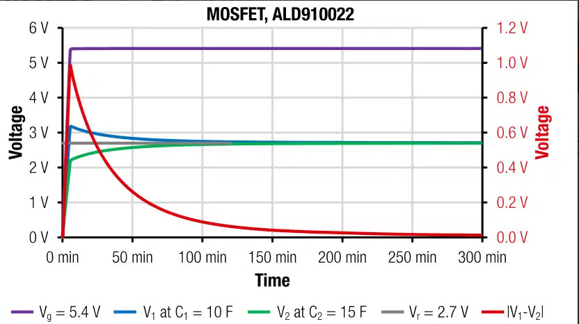
Figure 11: Time-dependent supercapacitor cell voltages V1, V2, and Vg as well as the voltage difference |V1 – V2| as measured for the active balancing with the ALD910022.
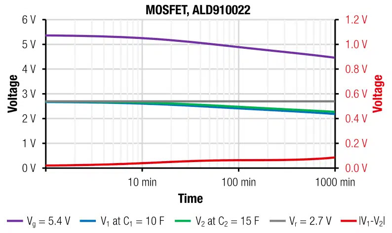
Figure 12: Measured self-discharge of supercapacitor balancing circuit with MOSFET. Graph shows time-dependent cell voltages V1, V2 and Vg as well as the voltage difference |V1 – V2| (corresponds to ordinate on right hand side)
The results of the self-discharge measurement in Figure 12 show that after 24h, the total cell voltage has decreased to about 4V. With this rate, tloss will be in the order of several days. A comparison to the maintained voltage measurement at the REDEXPERT online tool [10] suggests that the MOSFET does not significantly increase the self-discharge rate. We, therefore, conclude the circuit is suitable for long-term stand-alone applications.
Amplifier Active Balancing
For the active balancing with the amplifier OPA2677 (Texas Instruments), we utilized a circuit as given in Figure 13. The advantage of the OPA2677 is the relatively high output current of 500mA, which enables a fast balancing
The measured cell voltages in Figure 14 show an instantaneous balancing within the charging time, which is, in this measurement, about 3min. The balancing speed can be further increased by decreasing the damping resistor from 1Ω to 0.4Ω. With 0.4Ω, the balancing times of around 2min were reached. The trade off was a noticeable decaying oscillating behavior. The damping resistor at the output should not be below 0.4Ω to prevent oscillation of the output voltage. We found 1Ω to be the optimum between fast balancing and damping.
The overall power dissipation after 12h is 50mA ∙ 5.4V ≈ 270mW. The power is mainly dissipated via the supply terminals of the amplifier. This relatively high power consumption shows the main disadvantages of this type of strategy. It is fast, but it also has a large permanent power burn.
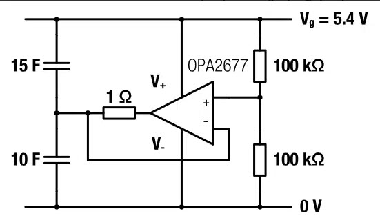
Figure 13: Active supercapacitor balancing circuit of OPA2677 as used for the measurements.
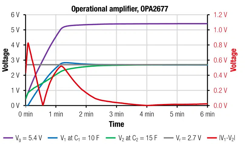
Figure 14: Time-dependent supercapacitor cell voltages V1, V2, and Vg as well as the voltage difference |V1 – V2| as measured for the active balancing with the OPA2677.
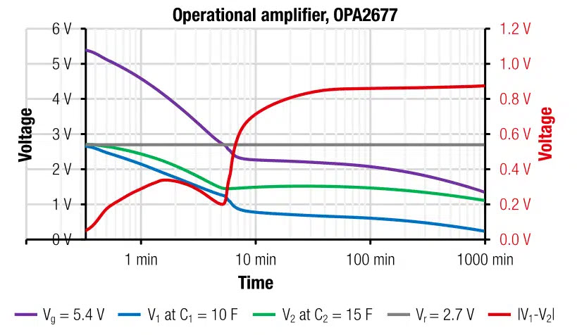
Figure 15: Measured self-discharge of supercapacitor balancing circuit with the OPA2677. The graph shows time-dependent cell voltages V1, V2, and Vg as well as the voltage difference |V1 – V2| (corresponds to ordinate on the right-hand side).
The results of the self-discharge measurement in Figure 15 indicate a half-life self-discharge time of tloss = 5min. Since we may only speculate about the voltage dependence of current losses at the terminals, we refrain from a mathematical estimation of tloss. We do not consider the circuit suitable for long term standalone applications.
Although the circuit always ensured a balanced charging, the losses via the supply channels are significant. We demonstrated, however, the feedback amplifier might work in principle. It is, in the end, the developer’s responsibility to find the best solutions for his application.
Active Balancing with DC-DC Converter
The evaluation board DC1887A utilizes the buck-boost SC charger and balancer LTC3128 from Analog Devices. It charges the SCs at a preset voltage of 4.2V. The board operates at a supply voltage of 5.5V. The measurement results in Figure 16 indicate a complete balancing after 1.5min. The overall power dissipation after 12 h is 0.1mA ⋅ 5.4V ≈ 0.5mW.
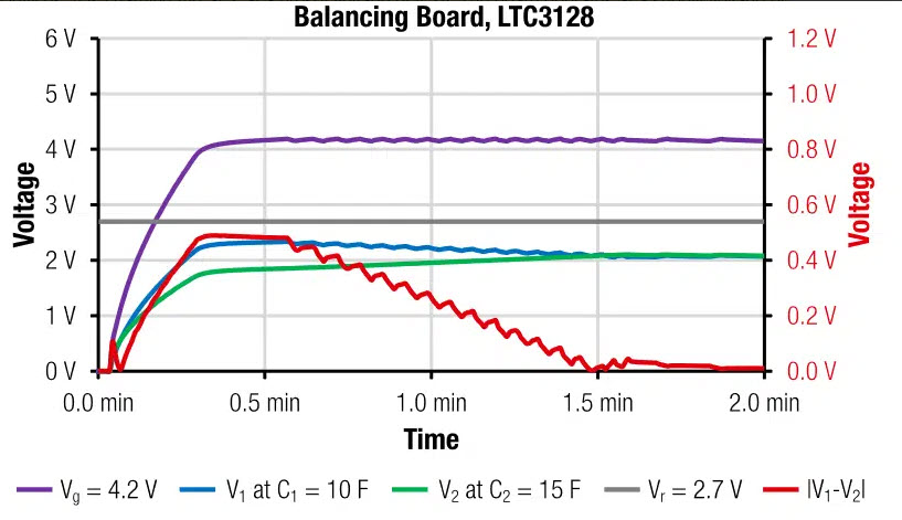
Figure 16: Time dependent cell voltages V1, V2 and Vg as well as the voltage difference |V1 – V2| as measured for the supercapacitor active balancing with the LTC3128.
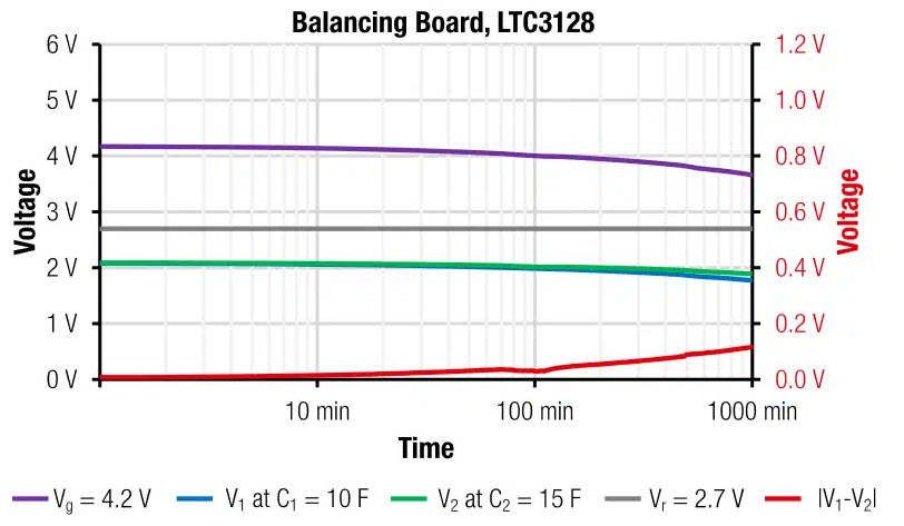
Figure 17: Measured self-discharge of supercapacitor balancing circuit with LTC3128. Graph shows time-dependent cell voltages V1, V2 and Vg and the voltage difference |V1 – V2| (corresponds to ordinate on the right-hand side).
- Miniature RF Connectors for high-performance testing - April 24, 2025
- Space-Grade components available for immediate delivery - April 10, 2025
- Managing EEE components for LEO and lower cost space missions - December 17, 2024

0 comments on Supercapacitors voltage measurements