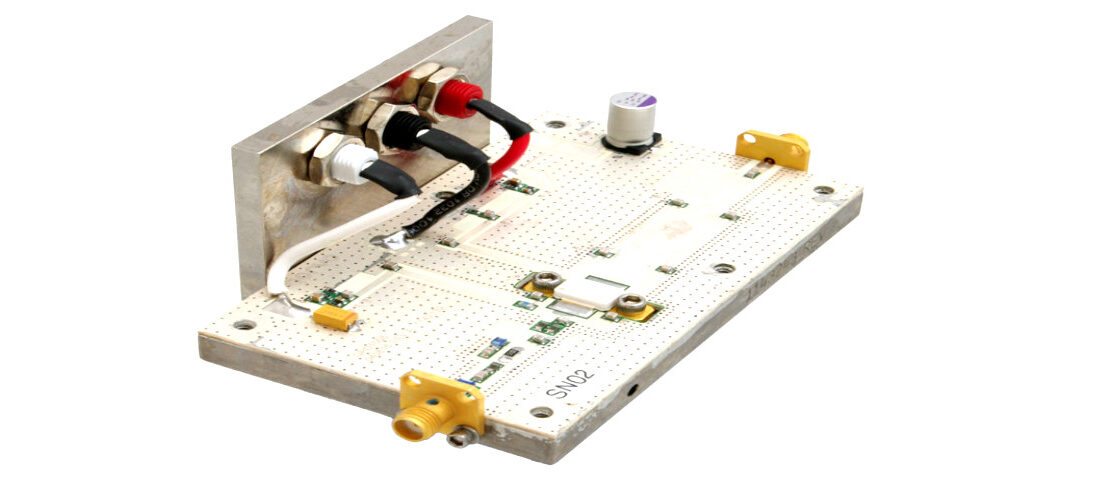
Temperature Stability Assessment of GaN Power Amplifiers
- Posted by Tomáš Zedníček
- On July 5, 2020
- 0
Linearity is one of the key power amplifier design parameter. Requirements for the best linearity of RF GaN power amplifiers can be achieved by two ways: use of optimum output impedance of the optimum linearity, this could, however, limit the output power and decrease efficiency. Or use optimum output impedance for maximum power output and define the working linearity region by the proper BIAS point setting and optimization.
GaN and SiC wide bandgap semiconductor technology have been used for past 15 years mainly in RF high-frequency applications with its main contribution to system designs with significantly reduced losses. The popularity of GaN systems for RF is rapidly increasing, RF GaN market is expected to grow at 22.9 % CAGR over 2017-2023, boosted by the implementation of 5G networks. [1]
Nevertheless, the GaN “revolution” is not only about the high RF frequencies. During the past recent years, the wideband semiconductors have reported achievement of over a 1000 V breakdown voltage that opens new challenges for high power industrial applications such as electric traction systems in trams, trolleybuses or high-speed trains, etc.
Temperature stability of power converters in a wide range of industrial applications may be of critical importance. A number of recent GaN power boards is using decoupling and BIAS matching tantalum capacitors due to its stability of capacitance value over a wide temperature range, stable capacitance with BIAS, no piezo noise sensitivity at small, low profile case sizes.
This article is sharing some tantalum capacitor design-in references linked with the recent GaN power system designs. Temperature stability from -30 °C to +70 °C of a typical GaN power amplifier with tantalum capacitor on board is evaluated in addition.
GaN Power Amplifiers – Overview
Telecom and defense markets will stay as the mainstay of the GaN industry. Due to the increasing pace of development of 5G networks, the telecom market will bring a huge opportunity for GaN devices. Compared with existing silicon LDMOS and gallium arsenide (GaAs) solutions, GaN devices can deliver the power/efficiency required for next-generation high-frequency telecom networks. Also, GaN’s broadband capability is a key factor for enabling important new technologies, such as multi-band carrier aggregation. At the same time, market volumes will increase faster because higher frequencies reduce the coverage of each base station, hence more transistors will be implemented. [1].
Linearity is one of the key GaN power amplifier design parameter. Requirements for the best linearity of RF GaN power amplifiers can be achieved by two ways: 1] use of optimum output impedance of the optimum linearity, this could, however, limit the output power and decrease efficiency. Or 2] use optimum output impedance for maximum power output and define the working linearity region by the proper BIAS point setting and optimization. This way requires a proper design of BIASing circuits and its stability in wide operating conditions. The same consideration is valid for a proper design of the gate BIAS level. [2]
Tantalum capacitors have become the favorite choice for BIAS decoupling capacitors in GaN power amplifiers, ensuring the stability of its electrical parameters at various conditions and keeping the GaN transistor working point within the high linearity region.
RF GaN reference designs with tantalum capacitors (for example, not exhausted list):
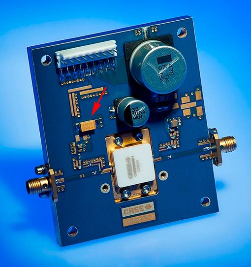
Fig.1. RF GaN Power Amplifier; image credit: Cree
- Nitronex NPTB00004 GaN 28 V, 5 W RF Power Amplifier for CW, pulsed, WiMAX, W-CDMA, LTE, and other applications from DC to 6 GHz. Tantalum capacitors of 10 μF 16 V has used at gate decoupling capacitors.
- Qorvo QPD1008 125 W, 50 V, DC – 3.2 GHz, GaN RF With 10μF 16V capacitors as gate BIAS decoupling capacitors.
The other Qorvo similar design and references with tantalum capacitors:
-
-
- QPD1008L DC – 3.2 GHz, 125 Watt, 50 Volt GaN RF Power Transistor
- QPD1009 DC – 4 GHz, 15 Watt, 50 V GaN RF Transistor
- QPD1010 DC – 4 GHz, 10 Watt, 50 V GaN RF Transistor
- QPD1015L DC – 3.7 GHz, 65 Watt, 50 V GaN RF Power Transistor
-
- Cree / Wolfspeed CGHV50200F 200 W, 4400 – 5000 MHz, 50-Ohm Input/Output Matched, GaN HEMT using 10μF 16V capacitors
The other Cree references with tantalum capacitors:
-
-
- CGH40006P 6 W, RF Power GaN HEMT
- CGH40010 10 W, DC – 6 GHz, RF Power GaN HEMT
- CGH40025 25 W, RF Power GaN HEMT
- CGH40045 45 W RF Power GaN HEMT
- CGH55030F1 / CGH55030P1 30 W, 5500-5800 MHz, 28 V, GaN HEMT for WiMAX
-
GaN High Power PFC Compliant Systems
The main power supplies used in telecom, server, and industrial power supply unit (PSU) systems convert AC line power to an isolated constant DC voltage output suitable for the loads the power: typically, 12 V for server PSUs, 48 V for telecom rectifiers, and 24 V for industrial PSUs. These main power supply system’s range typically from 1 kW to 5 kW. These systems require a front-end power factor correction (PFC) circuit to shape the input current of the power supply, so as to meet the power factor and current total harmonic distortion (THD) norms defined in IEC61000-2-3.
Requirements for PFC front ends have undergone considerable changes over the last few years due to increasing demands for smaller size and higher efficiency. The challenge to meet premium levels of more than 80 % standards calls for very-high efficiency over wide operating ranges of input and output. This need for high efficiency has generated considerable interest in bridgeless topologies for the PFC stage that can push the efficiency above 99%. Because of the need for both smaller size and higher efficiency, simpler topologies that use fewer components and can switch at higher frequencies are the current requirement in the PFC front end. The adoption of topologies using GaN power devices is relevant in this context. Ref. source [3] Texas Instrument TIDA system.
The industrial power supplies are operating at wide temperature range conditions at high-reliability expectation often in 7/24/365 non-interrupted continuous power operation mode. The component selection guide is thus an important part of the selection process. Capacitors can be considered as critical components that in case of short circuit failure may cause a fatal system malfunction error. Tantalum capacitors are providing high capacitance efficiency in small dimensions with stable electrical parameter over its long lifetime. Thus, reference guidelines of modern GaN power supplies are recommending the use of tantalum capacitors:
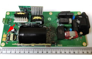
Fig. 2. Texas Instruments TIDA 00961 board, image credit: Texas Instruments
- Texas Instrument TIDA 00961 GaN 12 V, 1.5 kW for telecom, servers and industrial power supplies referring tantalum capacitors of 100 μF 16 V, 220 μF 16 V for bulk 12 V line stabilization [1], 4.7 μF 10 V on 3.3 V output stabilization.
- Texas Instrument LMG3410 600 V 12 A Integrated GaN Power Stage for solar power, battery chargers using tantalum capacitors of 33 μF 16 V as 5 V output capacitor
GaN Hi-Point of Low Controller
Another type of circuits where GaN transistors excel can be an example of a half-bridge point-of-load controller in a 48-V to 1-V application such as Texas Instrument LMG5200.
Texas Instruments evaluation board implements the 48-V to the 1-V converter as a single-stage hard-switched half-bridge with current-doubler rectifier. This topology efficiently supports a high step-down ratio while providing significant output current and fast transient response.
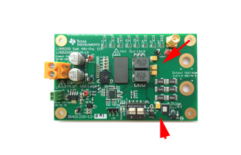
Fig. 3. Texas Instrument LMG5200 evaluation board, image credit: Texas Instruments
The used chip LMG5200 is an 80-V, 10-A half-bridge power stage using gallium-nitride (GaN) transistors. GaN offers superior switching performance to traditional silicon MOSFETs due to its lack of reverse-recovery effect and reduced input and output capacitance. By using a GaN module, this application achieves high efficiency while operating in a hard-switched configuration.
Four low ESR 150μF 6.3V polymer tantalum capacitors are used as high efficiency, high power filtering output capacitors in small 1210 tantalum B case size.
GaN board selection
QORVO QPD1008 has been selected as a typical representative board with tantalum capacitors on the input side and subjected to a temperature stability measurement at RICE, University of West Bohemia. The QPD1008 is a 125 W (P3dB) wideband unmatched discrete GaN on SiC HEMT which operates from DC to 3.2 GHz with a 50 V supply rail. The device is in an industry standard air cavity package and is ideally suited for military and civilian radar, land mobile and military radio communications, avionics, and test instrumentation. The device can support pulsed, CW, and linear operation. [4]
In measurement set up, this transistor was connected in the test board as an amplifier for the frequency range from 0.96 GHz to 1.215 GHz. The aim was to observe the influence of the C2 capacitor on the transistor behavior for different ambient temperature level. The C2 capacitor is tantalum capacitor (10 μF/16 V) recommended by the manufacturer in its reference datasheet – see Fig. 4 and Fig. 5.
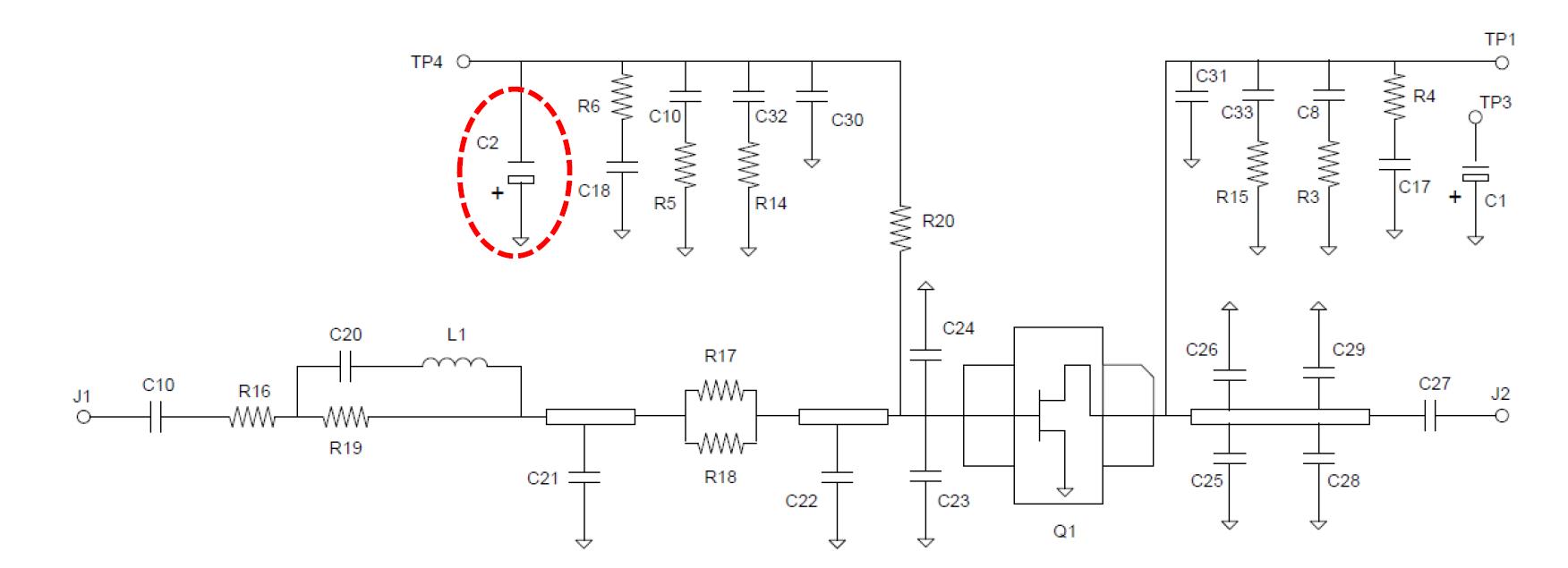
Fig. 4: Circuit diagram of GaN QPD1008 connection as an amplifier for frequency range from 0.96 GHz to 1.215 GHz; circuit image credit: Qorvo QPD 1008 datasheet
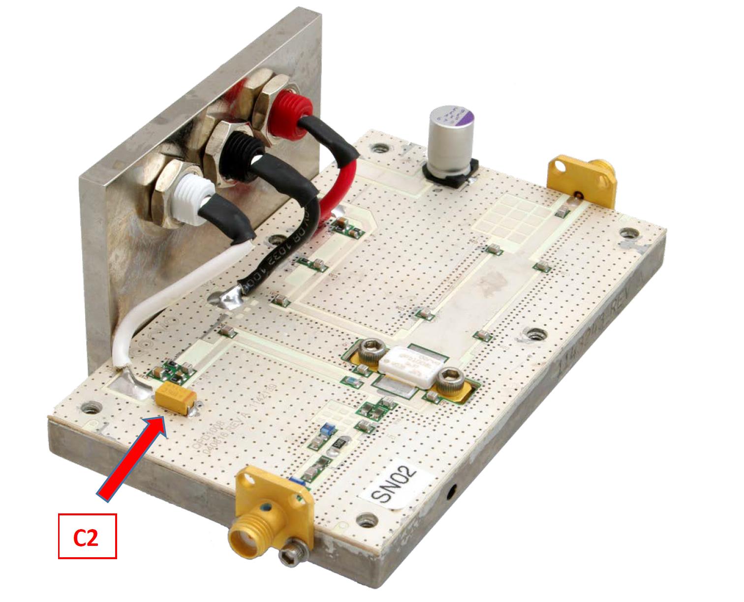
Fig. 5: GaN QPD1008 evaluation test board with C2 tantalum capacitor; image credit: EPCI
Measurement Setup
The measurement was performed at standard measurement conditions within the referenced datasheet operating conditions recommendations:
Bias and voltage setup: according to the recommendation in the datasheet
Input signal: sin wave, frequency of 1 GHz, power of 15 dBm
Ambient temperature: -30 °C; +25 °C and +70 °C
Measurement equipment:
- Spectrum analyzer Agilent N9320B
- Oscilloscope Tektronix MSO4104B
The spectrum analyzer was connected to the test board output via the attenuator with attenuation of 30 dB. C2 tantalum capacitor waveforms were measured by oscilloscope and compared at different temperatures. The test board was inserted into the climatic chamber. Before the measurement, the test board was conditioned at least 30 minutes at the desired temperature (-30 °C, +25 °C, and +70 °C). The spectrum of output signal was measured and compared.
GaN Power Amplifiers – Measurement Results
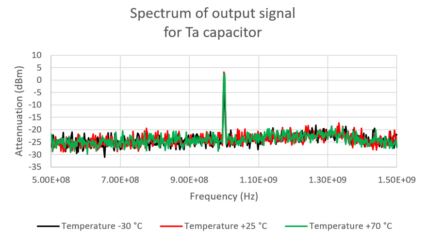
Figure 6, 7 and 8 present measured waveforms and its FFT analyses on C2 tantalum capacitor position at three different temperatures: -30 °C, 25 °C and +70 °C. Spectrums of the output signals of GaN test boards were measured and compared – see figure 9 and 10.
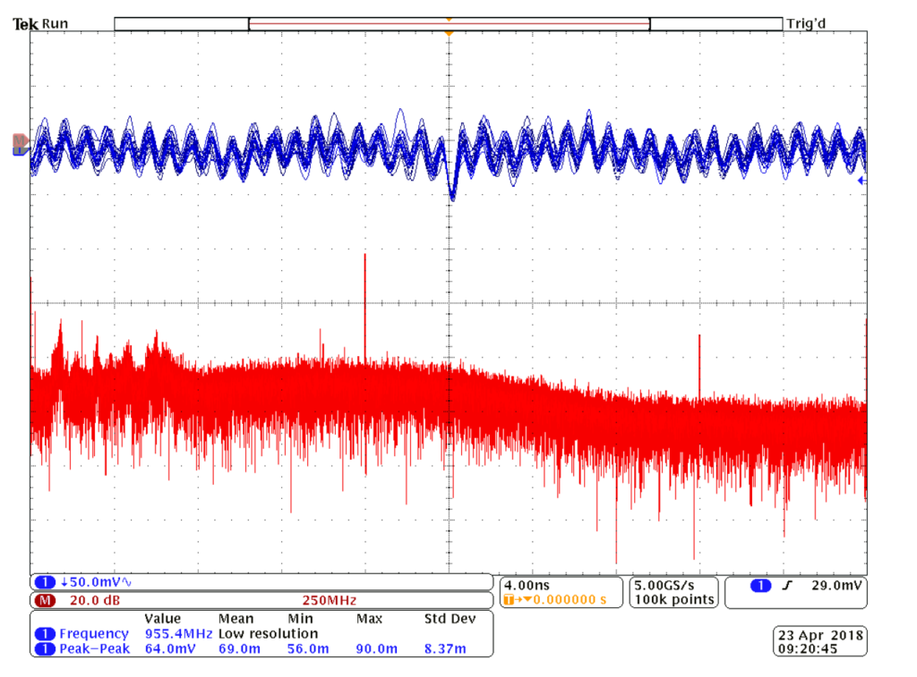
Fig. 6: Waveform on C2 tantalum capacitor at -30 °C and its FFT analysis; chart credit: UWB
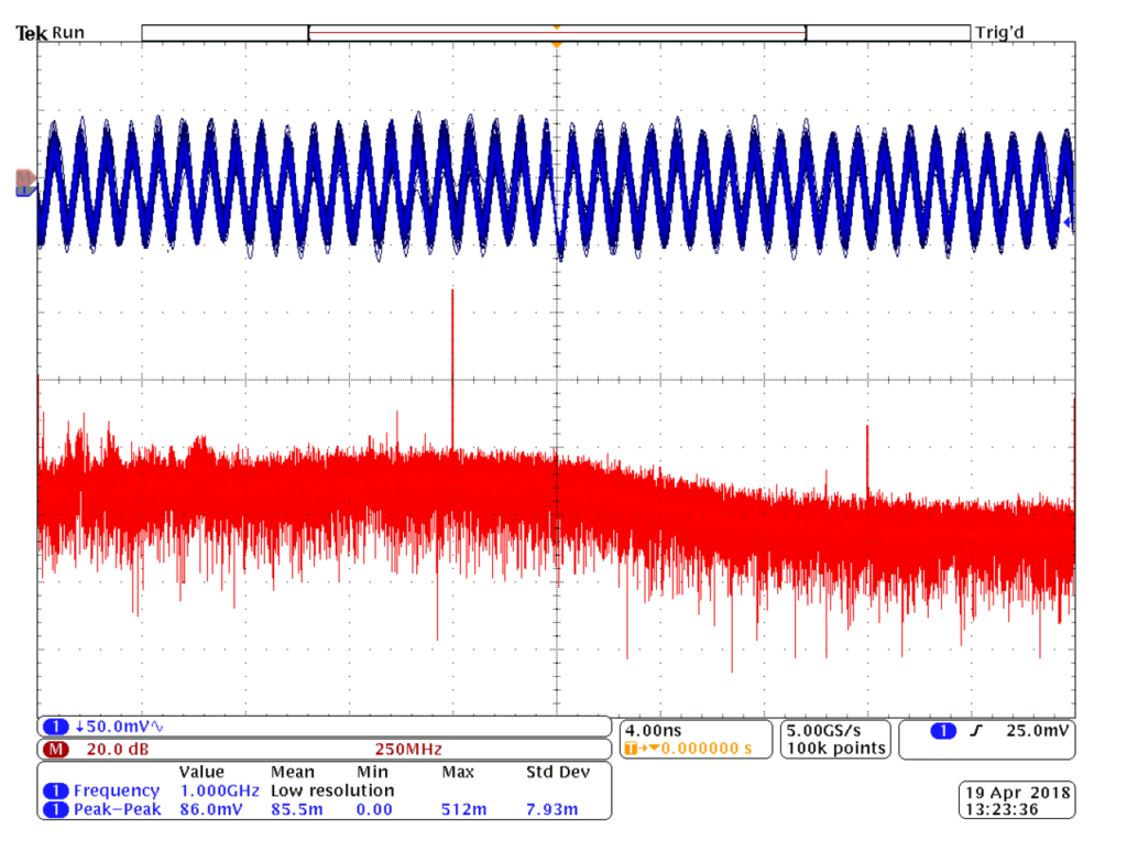
Fig. 7: Waveform on C2 tantalum capacitor at +25 °C and its FFT analysis; chart credit: UWB.
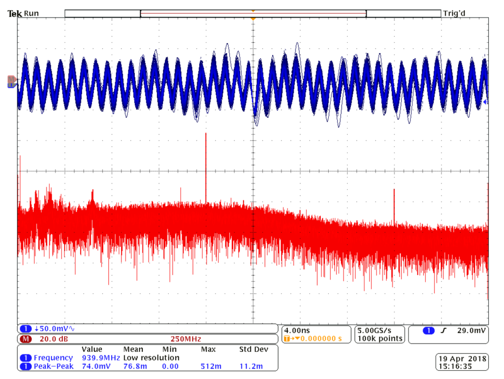
Fig.8. Waveform on C2 tantalum capacitor at +70 °C and its FFT analysis – tantalum capacitor.
Spectrums of the GaN test board output signals for different temperatures.
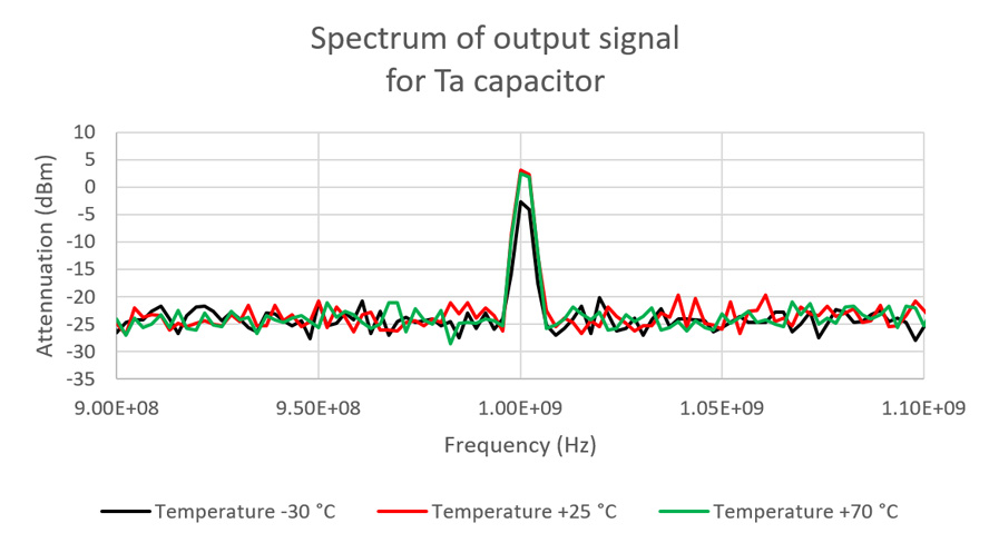
Fig.10. Spectrum detailed view from Fig. 9. around the test signal frequency.
Measurement Summary
There are practically no measurable differences in output signal stability of the tested RF amplifier board in operation at +25 °C and +70 °C temperatures. Some output signal drops about 5 dBm test frequency attenuation is visible in the measured spectrums at an ambient temperature of -30 °C. Nevertheless, such a shift within 5 dBm can still be considered as a very good stability performance of the tested GaN RF power amplifier at the referenced conditions.
References
[1] semiconductor-today press release; January 2018;
[2] Texas Instrument TIDA 00961 GaN 12V, 1.5KW design-in note; January 2018; http://www.ti.com/lit/ug/tidudt3/tidudt3.pdf
[3] Markos.A.,Z.; “Efficiency Enhancement of Linear GaN RF Power Amplifiers Using the Doherty Technique”; 2009; Kassel university press GmbH; ISBN online: 978-3-89958-623-7
[4] Qorvo QPD1008 125W, 50V, DC – 3.2 GHz, GaN datasheet; https://www.qorvo.com/products/p/QPD1008
Co-authors:
R.Demcko, M.Weaver, D.West, AVX Corporation, Fountain Inn, SC, USA
T.Blecha, F.Steiner, J.Svarny, R.Linhart, RICE, University of West Bohemia, Pilsen, Czech Republic
- Why low ESR matters in capacitor design - May 24, 2021
- Voltage and Frequency Dependence on Resistors - March 6, 2021
- Permeability concept in Inductors - March 4, 2021

0 comments on Temperature Stability Assessment of GaN Power Amplifiers