PCB Trace Impedance Measurement and Simulation
- Posted by doEEEt Media Group
- On December 27, 2020
- 0
This article investigates the impedance of the three standard passive circuit components (R, L, and C) as well as the frequency response of a PCB trace. It is shown that a PCB trace can be modeled as a resonant RLC network just like the standard components and effectively constitutes the fourth circuit component whose frequency behavior directly effects the impedance of the resistors, inductors, and capacitors on a PCB.
1. Component Models and Simulations
Actual circuit components exhibit non-ideal effects that can be modeled by augmenting the ideal model with a parasitic resistance, inductance, and capacitance. The parasitics for the three standard components (R, L, and C) considered in this section come from the component itself and not from the connecting traces. The parasitics associated with a PCB trace considered in this section come from the trace itself and not from the other circuit components.
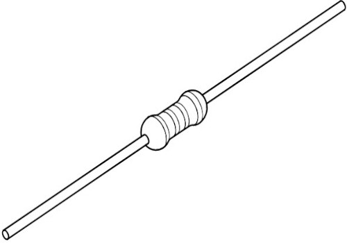
- Resistor
Circuit model and the impedance vs. frequency curve (straight-line approximation) for a resistor and its parasitics (with no traces attached) are shown in Figure 1.
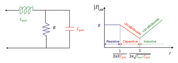
Figure 1: Resistor circuit model and its impedance curve
The parasitic inductance and capacitance in Figure 1 are inherent to the component itself and the fabrication method and are not attributed to the connecting traces. Figure 2 shows the simulation results for a 300-Ω surface mount resistor together with its realistic parasistics (simulation is run between 1 MHz and 1 GHz).
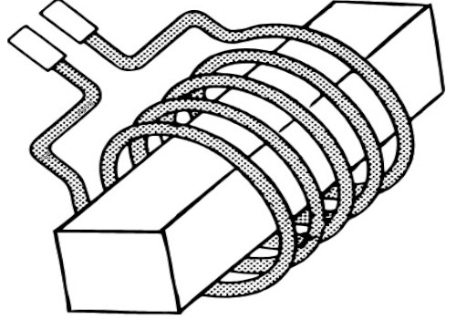
- Inductor
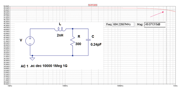
Figure 2: Resistor with its parasitics – impedance vs. frequency (no connecting traces)
The low-frequency impedance stays at 49.5 dB and drops by 1 dB at 1 GHz. The self-resonant frequency is well above 1 GHz and thus not shown in the simulation. This simulation result will be confirmed in the measurement section.
Circuit model and the impedance vs. frequency curve for an inductor with its parasitics (with no traces attached) are shown in Figure 3.
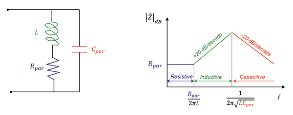
Figure 3: Inductor circuit model and impedance curve impedance vs. frequency (no connecting traces)
Figure 4 shows the simulation results for a 220-nH inductor together with its realistic parasistics.
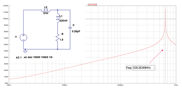
Figure 4: Inductor with its parasitics – impedance vs. frequency (no connecting traces)
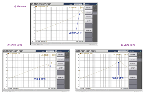
The self-resonant frequency of the inductor is 638.2 MHz – this result will be confirmed in the measurement section.
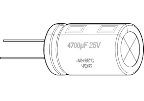
- Capacitor
Circuit model and the impedance vs. frequency curve for a capacitor with its parasitics (with no traces attached) are shown in Figure 5.
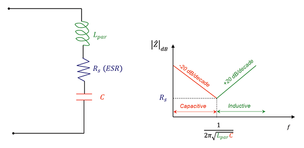
Figure 5: Capacitor circuit model and impedance curve
Figure 6 shows the simulation results for a 120-pF capacitor together with its realistic parasistics.
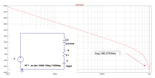
Figure 6: Capacitor with its parasitics –impedance vs. frequency (no connecting traces)
2. Impedance Measurements
The self-resonant frequency of the capacitor is 995.2 MHz – this result will be confirmed in the measurement section.
- PCB Trace
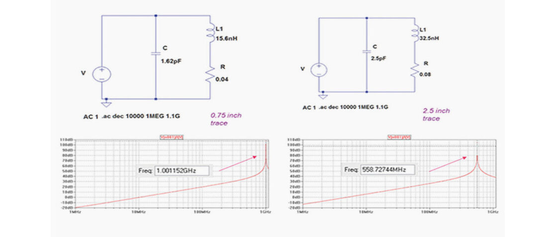
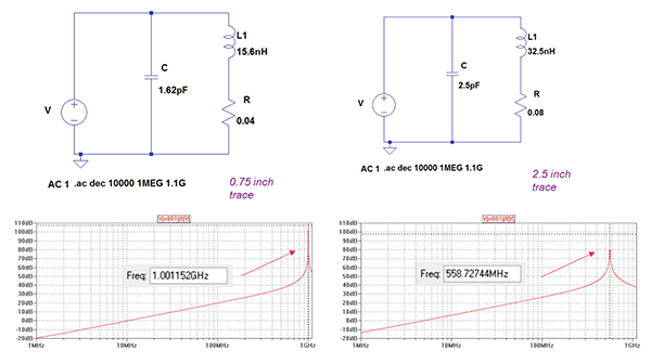
Figure 7 shows the circuit models and the impedance curves for two PCB traces of length 0.75 and 2.5 inches, respectively.
Figure 7: PCB traces with their parasitics – circuit model and impedance vs. frequency (no components attached)
Comparison of these curves with the one in Figure 4 reveals that an unpopulated PCB trace acts as an inductor! The longer trace has larger inductance and hence its self-resonant frequency is lower than that of the shorter trace.
These are two very important observations since in any practical circuit, the standard three passive components (R, L, and C) will be connected to other components with PCB traces. These traces will act as the fourth circuit component whose impact will depend on its trace length. The measurement section will illustrate this impact.
2.1 PCB Trace
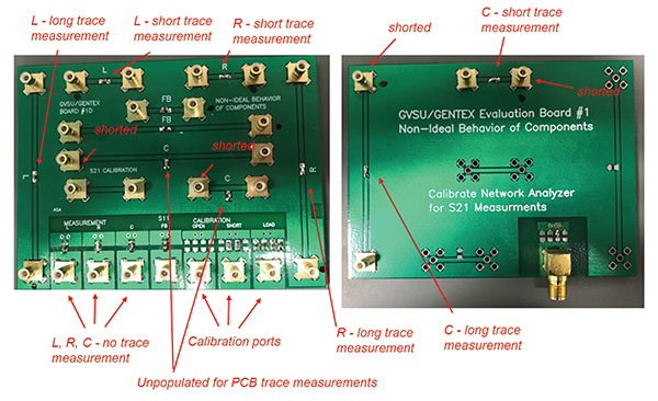
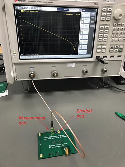
Figure 10 shows the impedance measurement of two unpopulated PCB traces of length 0.75, and 2.5 inches, respectively.
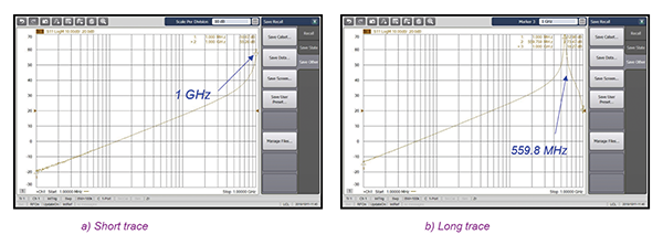
Figure 10: PCB Trace – impedance measurements: a) short trace, b) long trace
2.2 Resistor
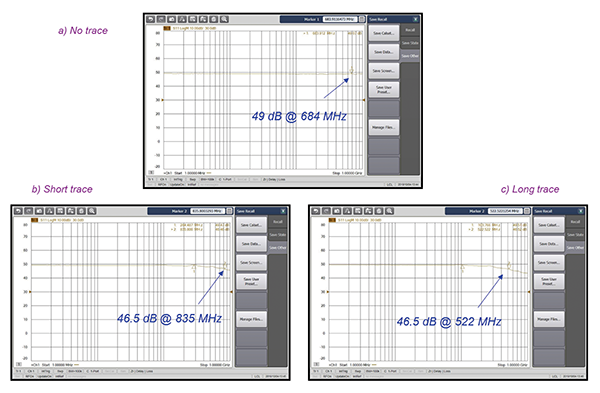
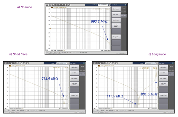
Figure 11 shows the impedance measurement of a 300-Ω resistor with no connecting traces and with the PCB traces of length 0.75, and 2.5 inches, respectively. (Resistor used is Stackpole Electronics, Inc. RMCF0805JT300R).
2.3 Inductor
Figure 12 shows the impedance measurement of a 220-nH inductor with no connecting traces and with the PCB traces of length 0.75, and 2.5 inches, respectively. (Inductor used is Murata, LQG18HHR22J00).
2.4 Capacitor
Figure 13 shows the impedance measurement of a 120-pF capacitor with no connecting traces and with the PCB traces of length 0.75, and 2.5 inches, respectively. (Capacitor used is Murata, CGM1885C1H121JA16).
References
- Bogdan Adamczyk, Foundations of Electromagnetic Compatibility with Practical Applications, Wiley, 2017.
- Adamczyk, B., Teune, J., “Impact of a Trace Length on Capacitor Frequency Response,” In Compliance Magazine, March 2018.
- Bill Spence and Pete Vander Wel, “Designers of the PCB used for impedance measurements,” Gentex Corp, 2008.
Source: InCompliance Mag article
by Bogdan Adamczyk and Jim Teune in EMC Concepts Explained.
- Miniature RF Connectors for high-performance testing - April 24, 2025
- Space-Grade components available for immediate delivery - April 10, 2025
- Managing EEE components for LEO and lower cost space missions - December 17, 2024


0 comments on PCB Trace Impedance Measurement and Simulation