Non-Linear Resistors: Thermistors, Varistors, Memristors
- Posted by doEEEt Media Group
- On June 22, 2023
- 0
Non-linear resistors are resistive components where its resistance is not behaving linearly with parameters such as voltage, current (varistors), temperature (thermistors), or it depends to the previous stage (memristors).
The non-linear resistance behaviour is successfully used to get specific features like sensors, limiters, ESD protection, self-balancing temperature stabilisation etc., using still a relatively simple and reliable passive component.
- thermistors
- varistors
- memristors
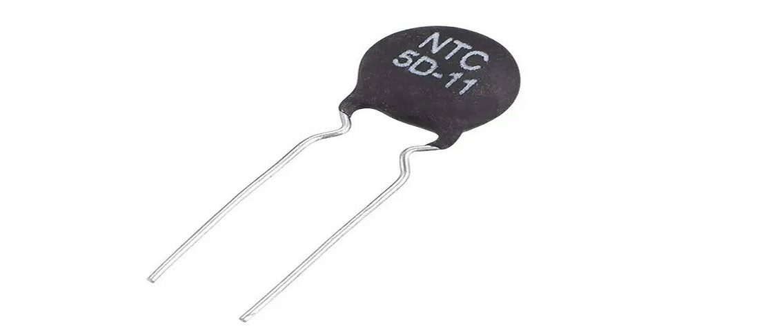
NTC Thermistors
Simplified, the thermistor material consists of doped granule compounds containing various oxides that, using binders, have been pressed to a desired shape and then sintered. The terminals are inserted into the resistor body or soldered to metallized surfaces. There are several encapsulation types.
Designs
Thermistors exist as rods, discs, beads covered with lacquer, epoxy, glaze or melted glass, and SMDs.
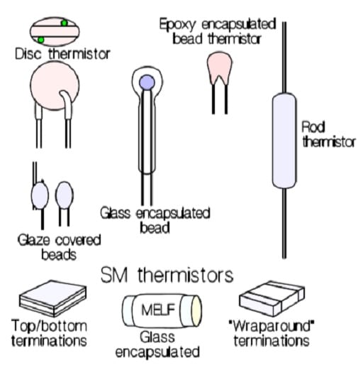
Figure 1. Thermistor design examples.
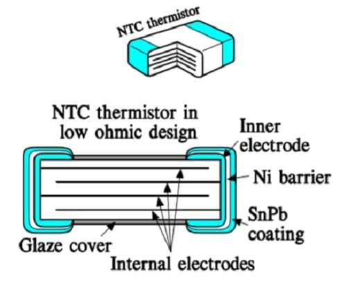
Figure 2. Construction of a low ohmic chip thermistor.
SMD thermistors in low ohmic designs are made with several internal electrodes, as shown in Figure 2. The reduced resistance is achieved by a construction that connects “resistor elements” in parallel inside the thermistor body.
Temperature Dependence and Tolerances
NTC stands for negative TCR (Negative Temperature Coefficient). The temperature dependence is strong and exponential and follows the formula:
![Thermistor temperature dependence equation [1]](https://www.doeeet.com/content/wp-content/uploads/2023/06/thermistor-temperature-dependence-with-time-equation-4.jpg)
Thermistor temperature dependence equation [1]
The material constant A determines the resistance and B its temperature dependence, i.e. the slope of the resistance–temperature curve. T means the temperature in Kelvin (°C + 273). If we apply the formula [1] on a reference temperature T0 and a general temperature T and combine the two expressions, we obtain the formula
![thermistor reference temperature dependence equation [2]](https://www.doeeet.com/content/wp-content/uploads/2023/06/thermistor-reference-temperature-dependence-equation.jpg)
thermistor reference temperature dependence equation [2]
The constant B generally is determined by measurements at 25 and 50 °C. It usually has values between 2500 and 5000. The value varies a little with temperature. Hence the ≈ symbol in the formulas. The thermistor material shrinks strongly during the sintering process, which causes great difficulties in keeping the tolerances on both the R25 and the B values within specified limits. The B value is stated with tolerances that usually are 5 %. The reference value R0 relates to 20 or 25 °C and has tolerances of 5, 10 or 20 %. However, sawing already sintered chips to close dimensions increases the accuracy considerably. R25 tolerances of 0.2⋅⋅⋅1 % no longer are exclusive, nor are tolerance of 1 % on the B value. The result of these superimposed tolerances looks like the illustrations in Figures 3. to 5.
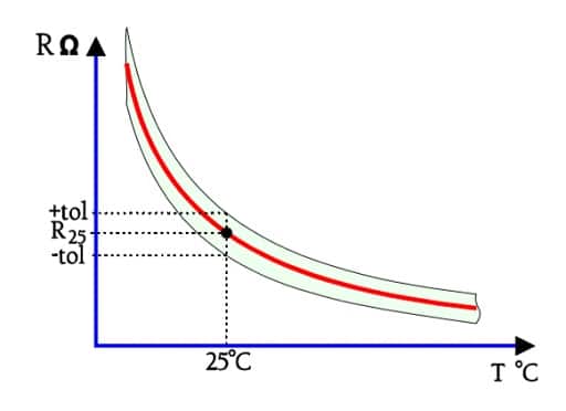
Figure 3. Thermistor tolerances at the reference temperature T25.
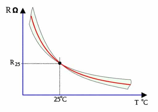
Figure 4. Thermistor B tolerance effect.
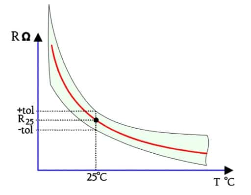
Figure 5. The combined effect of the R25 and B thermistor tolerances.
For more accurate applications, two or more points on the Resistance/Temperature curve – abbreviated R/T curve – are specified a so-called curve-tracking application. The B tolerances, then, are of less importance. The tolerances of such a two or three-point sensor may be stated either as a resistance deviation ∆R in per cent of R or as a temperature deviation ∆T in °C at the temperatures in question (Figure 6). In the latter case, we must calculate ∆R using the temperature coefficient α in the Formula [3].
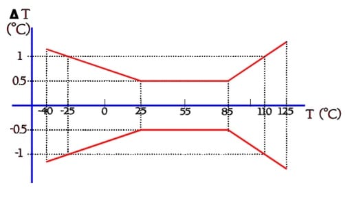
Figure 6. Example of alternative thermistor tolerance specification using a so-called butterfly curve.
Slope and Temperature coefficient
The B value determines the slope of the R/T curve for an NTC thermistor. Sometimes the temperature coefficient an (also called α) is also specified. If we derive the expression in Equation [1], we obtain:
![thermistor temperature coefficient equation [3]](https://www.doeeet.com/content/wp-content/uploads/2023/06/thermistor-temperature-coefficient-equation-3.jpg)
Thermistor temperature coefficient equation [3]
Compared to the general resistor TCR formula, where TCR = 1/R x ∆R/∆T, we find the same basic expression as for α. As follows from Equation [3] α varies strongly with temperature. Around 25 °C α usually has values between –3 and –5.5%/°C. Yet another way of specifying the slope of the R/T curve is by using resistance ratios. For example, the ratios of R0/R50 or R25/R125 are compared. The ratios are stated with tolerances.
Self-Heating Effects
The self-heating of the NTC thermistor influences the resistance. If we apply a voltage over the thermistor, the current at the beginning rises linearly according to Ohm’s law. But the resistance starts decreasing as soon as the internal power generates palpable heat. The further voltage rises gradually force resistance reductions that occur faster than the current increases. The V/I curve starts declining (Figures 7. and 8.).
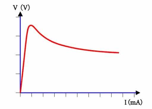
Figure 7. The self-heating effect on the V/I curve of an NTC thermistor
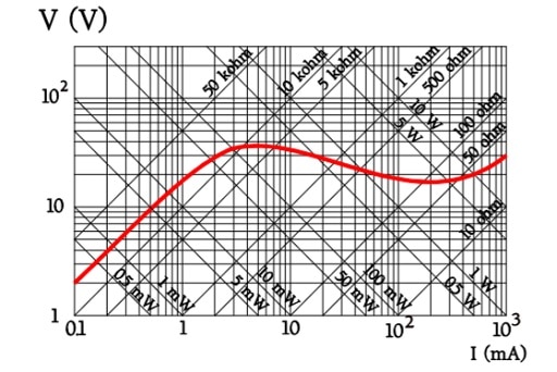
Figure 8. NTC thermistor example of the V/I diagram in log-log scale and power and resistance grading.
The example in Figure 8. helps us realize how the parameters V, I, P and R belong together.
Thermal Cooling Time Constant, Heat Capacity and Dissipation Factor
Two parameters are associated with Figure 8., namely, time and temperature. Size, shape and surrounding medium influence the velocity with which the temperature is changed. A measure of the change velocity is the thermal time constant, t. It is specified for an in-still-air freely mounted thermistor body under zero power conditions. It is defined as the time required for the temperature to change by 63.2% – exactly (1-1/e) – of the difference ∆T between the initial and final body temperature, T0 respectively T∞ (Figure 9).
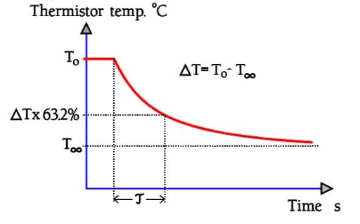
Figure 9. Time constant t of an NTC thermistor
Thermistor temperature dependence equation [1]
t also can be deduced from two material constants, the heat capacity H (J/°C) and the dissipation factor D (mW/°C).
![thermistor thermal cooling constant equation [5]](https://www.doeeet.com/content/wp-content/uploads/2023/06/thermistor-thermal-cooling-constant-equation-5.jpg)
thermistor thermal cooling constant equation [5]
The heat capacity describes how many Joules (Ws) that have to be conveyed to the thermistor body in order to raise its mean temperature by 1 °C. The dissipation factor D is expressed in mW/°C (or mW/K) and is specified as the power that raises the mean temperature of a thermistor body by 1 °C (or 1 K) when freely mounted in still air. The power dissipation capability, of course, can be increased by means of fans, heat sinks or another cooling medium, for example, a suitable liquid. In that case, one obtains a practical time constant. If the thermistor is placed in a suitable liquid the time constant is decreased drastically. Among other things, this is utilized in production control. The thermistor is immersed into a precise temperature-controlled bath and thus in a very short time is conveyed to the stable measurement temperature.
Thermistor Application / Choice of Type
We can distinguish three main groups of applications:
- The temperature dependence of resistance R = f(T) is utilized. The temperature then may be determined
- by the surroundings
- or by the internal power of the thermistor.
- The time dependence R = f(t) is utilized, i.e. we use the material’s inherent thermal inertia.
- The typical NTC characteristics of the material are utilized. When we choose a thermistor, we have to consider the following requirements
- Environment and encapsulation requirements. Glass, glaze cover, lacquer/epoxy, no encapsulation.
- Temperature range.
- Shape and design. Chip/SMD, rod, disc or bead thermistor.
- Soldering, spot welding or glueing.
- Reference temperature R25 and temperature coefficient α (-B/T2).
- Tolerance requirements on R25 and B value. Is it a point-matching or a curve-tracking R/T application?
- Power dissipation a) without perceptible heating. b) with maximum change in resistance value.
- Thermal time constant τ.
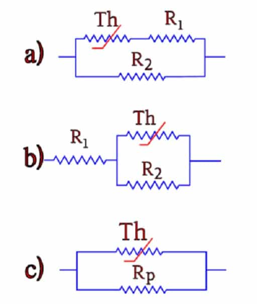
Figure 10. Correction circuits for the R/T characteristic of NTC thermistors.
Linearizing the R/T characteristic
If we want a temperature dependence with a particular slope of the R/T characteristic over a broader temperature range, it is usually difficult to find a suitable curve shape. However, by means of fixed resistors combined with the thermistor, it is possible to adjust the R/T curve in the desired direction. Figure 10. shows some examples of simple circuits to do this.
With alternative c) one may obtain an interesting solution by dimensioning Rp according to Equation [6] below. The resulting parallel resistance gives a curve that intersects a straight line in three points, as shown in Figure 11.
![thermistor linearizing correction resistor equation [6]](https://www.doeeet.com/content/wp-content/uploads/2023/06/thermistor-linearizing-correction-resistor-equation-6.jpg)
thermistor linearizing correction resistor equation [6]
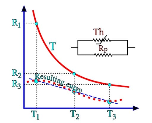
Figure 11. Linearizing the R/T curve of an NTC thermistor.
Failure Modes
Thermistors often have very small sizes and high resistance values. They are sensitive to every “disturbance” in the material. The terminal area is an exposed part of the body, especially for small sizes. If the body isn’t encapsulated in such a manner that any lead bendings are mechanically unloaded before the entrance to the thermistor body, it is easy to create small cracks around the lead entrance. With those cracks, the resistance is changed; there also is left a way for moisture and liquids to penetrate the body.
Glaze-covered beads and uncoated discs with terminals soldered direct on top of metallized pads are examples of vulnerable designs. Uncoated disc thermistors are not recommended for use in conductive liquids and aggressive gases. The sintered material sometimes undergoes settlings in the crystalline structure. Such events manifest as sudden resistance changes of 3 to 10 % and may be released by heat, temperature changes and mechanical shocks. The failure rate for non-treated delivery lots varies between 30 to 60 %. The cure is a burn-in process that usually is performed as a heat treatment.
Bead thermistors encapsulated in a melted glass body often have small sizes and corresponding thin leads, consisting of alloys that often are difficult to solder. In such events, leads intended for spot welding may be the only solution. Caution. Never try to connect NTC thermistors in parallel to increase the power dissipation capability. The thermistor that, for the moment, has the lowest resistance will get a higher current load, a stronger self-heating, a greater resistance decrease, an even higher current load etc. until the avalanche effect destroys the component.
Reliability
The reliability of NTC thermistors today is regarded as good. It depends not least on serious manufacturers with Statistical Process Control (SPC) based programs for manufacture and verified type qualifications. If we determine that the components are burn-in treated and if we purchase them with hermetic seals, i.e. glass or glass/metal housings, the reliability of such thermistors should be classified in the same group as fixed metallized film resistors.
SMD thermistors eliminate some of the problems connected with sensitive lead terminals. Initially, there were some solderability problems, but today they may be regarded as overcome. We now have got a component that structurally resembles the ceramic chip capacitor, however, with fewer sources of error. The stratified low resistance variant has its electrodes embedded in the material and may, from a reliability aspect, be comparable to the homogeneous type.
Read more about thermistors measurement system configurations, NTC vs PTC thermistors vs RTD resistor temperature detectors in this article: Thermistor-Based Temperature Sensing System Explained (passive-components.eu)
Nuclear radiation
Tests with radioactive radiation in the form of neutron, β and γ radiation show that thermistors can withstand high intensities without any effects on the characteristics.
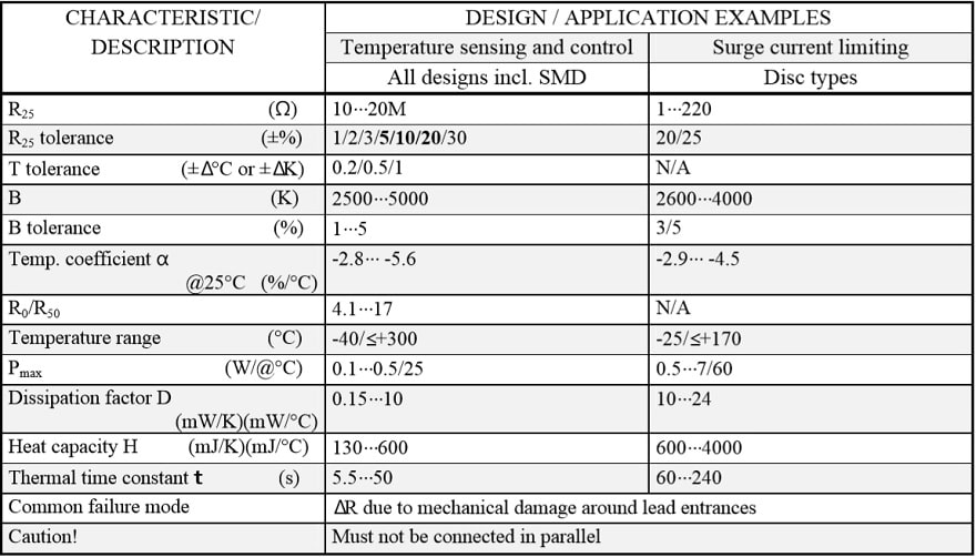
Table 1. NTC THERMISTORS CHARACTERISTICS
Varistors
Varistor stands for Variable Resistor. It’s a voltage nonlinear resistor/voltage-dependent resistor. It is an element that changes its resistance value depending on the applied voltage. This feature is mostly used to protect electronic devices from abnormal voltage, such as lightning surge and static electricity. Unlike thermistors, it has no practical time delay of its function.
Function and Design
Just as thermistors, the varistor is fabricated from a compressed and sintered powder compound that consists of silicon carbide (SiC) or zinc oxide (ZnO). The ZnO varistor has superior characteristics and predominates today in all manufacture. This section deals with ZnO varistors only. If we sinter zinc oxide together with other metal oxide additives, a polycrystalline ceramic is formed. In the intergranular boundaries of the zinc, oxide grains are formed P-N junctions with semiconductor characteristics – so-called Double Schottky Barriers – with rectifying characteristics. Each ZnO grain with adherent boundaries is a miniature varistor with a symmetrical V/I characteristic. The grain compound can be regarded as a conglomerate of “microvaristors” connected in series and parallel. Thus the load and energy absorption capability in that way will be superior to conventional semiconducting elements. The power generation exclusively will occur in the thin P-N boundary, while in the varistor, it takes place in all the microvaristors distributed homogeneously in the whole body.
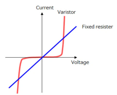
Figure 12. Example of V/I characteristic of a single varistor element.
The V/I characteristic of an elementary varistor may look like the one in Figure 12. Other manufacturers may have somewhat modified voltage values. The number of microvaristors connected in series and parallel determines the electrical characteristics of the varistor. Suppose we connect 10 grains in series with a part according to the figure. In that case, we get a varistor with a thickness of 10 grains and a varistor voltage of 30 V. Varistors are shaped and encapsulated approximately as the thermistors.
Of the different designs, discs are predominant, with radial leads and a variety of encapsulations, or with whole, metallized surfaces intended for series connection by piling the separate varistors. Encapsulations, for example, lacquer or the like, require high tensional stability and resistance against washing agents. A specific tubular connector design should also be mentioned for the uncovered types. At manufacturing, the goal is a grain compound with a regular structure, especially in high voltage/ high energy varistors.
An irregular structure impedes heat conduction and may lead to the uneven current distribution, occurring Hot Spots, and local material degradation. In low-voltage applications, homogeneity is of vital importance. Combining a multi-electrode construction and small, uniform grains has created the multilayer varistor (MLV), preferably used as SMD, intended for low-voltage applications.
These MLVs are manufactured similarly to multilayer ceramics (MLCCs). The electrodes are screen printed with thick film ink on the zinc oxide layers; the layers are stacked into a pile with the desired number of layers. The stack is then sintered to a monolithic body and finally supplied with terminations fired onto the body ends. Silver or silver/palladium is used as termination metal in old and military styles (Figures 13. and 14.), while BME nickel electrodes are today’s mass volume types. Plating of a nickel barrier requires due to the conducting zinc oxide unique processes, which deviate from the conventional electroplating.
Multilayer SMD designs are produced in EIA sizes from 0201 to 2220.
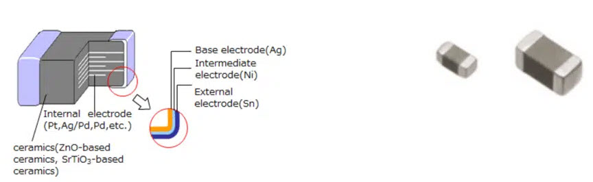
Figure 13. construction of multilayer SMD varistor; source: Panasonic
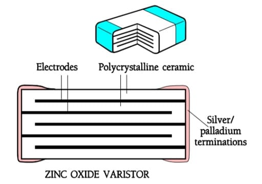
Figure 14. Schematic of a AgPd chip varistor in multilayer technique.
Some Definitions
Maximum working voltage
Maximum working voltage = the maximum voltage which continuously may be applied across the varistor.
Varistor voltage
The varistor voltage = the voltage across the varistor when a current of 1 mA is passed through the body.
Maximum clamping voltage
By maximum clamping voltage, we mean the peak voltage across the varistor when it is subjected to a specified peak pulse current with a specified waveform. A common test pulse is the IEC-specified so-called 8/20 pulse with a specified current intensity.
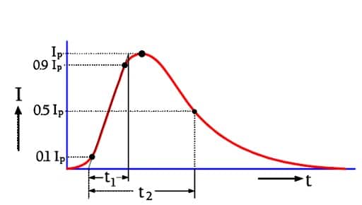
Figure 15. Standard thermistor test current pulse according to the IEC 60 with t1 = 8 µs and t2 = 20 µs.
Maximum transient peak current
The maximum current that may be allowed through a varistor depends on pulse shape and pulse width, repetition frequency and number of cycles. A starting point for the pulse capability is given by the maximum peak current of 8/20 shape that changes the varistor voltage with a maximum 10 %R
Varistor V / I Characteristic
The V/I curve of the elementary varistor is in Figure 12. differs slightly from that of the practical varistor that in the normal operation region might be approximated to
![varistor voltage dependence equation [7]](https://www.doeeet.com/content/wp-content/uploads/2023/06/varistor-voltage-dependence-equation-7.jpg)
varistor voltage dependence equation [7]
where:
C = varistor voltage at 1A.
I = actual working current.
β ≈ 0.03.
A typical V/I characteristic is shown in Figure 16.
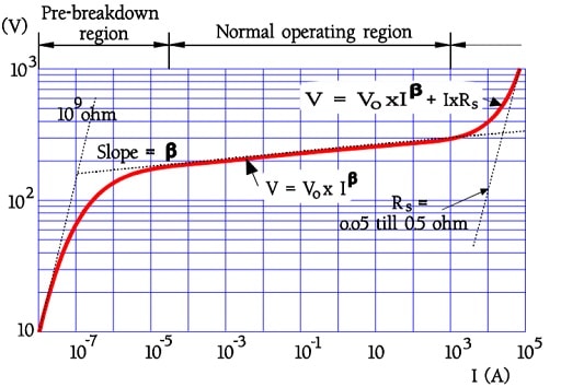
Figure 16. Typical V/I curve of a varistor
The V/I curve of a varistor has tolerances. When the leakage current is specified one presupposes the highest possible current at a certain voltage. The clamping voltage – the one occurring across the varistor when subjected to transients – is specified as the highest possible at a certain current. Thus the specifications are controlled by the unbroken line in Figure 17. Practical, standard-based limits for the varistor are shown in Figure 18.
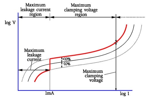
Figure 17. Specified regions and limits for a varistor.
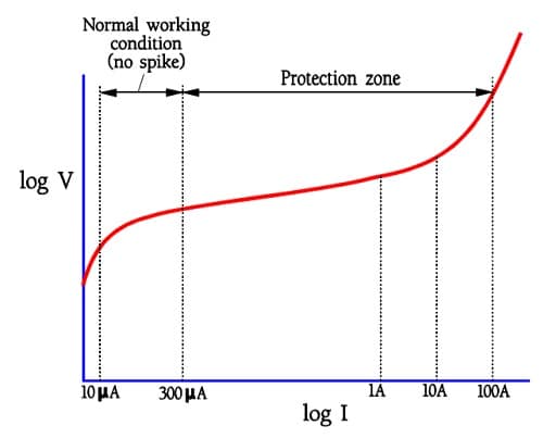
Figure 18. Definitions of the varistor curve.
Principles of Varistor Voltage Limitation
If the varistor is to operate as a voltage limiter a series impedance is required in the circuit. Common straight conductors have both resistance and inductance (≈ 1nH/mm) and provide themselves a certain protection. Practically, however, the problem is solved by a series resistor of some hundred(s) of ohms (Figure 19.).
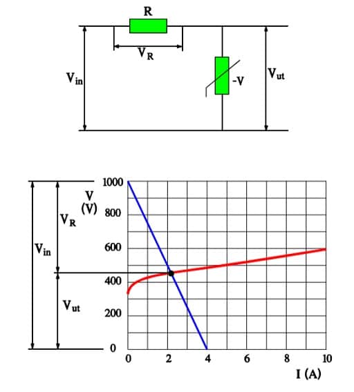
Figure 19. An example of voltage limitation by a varistor + series resistor combination.
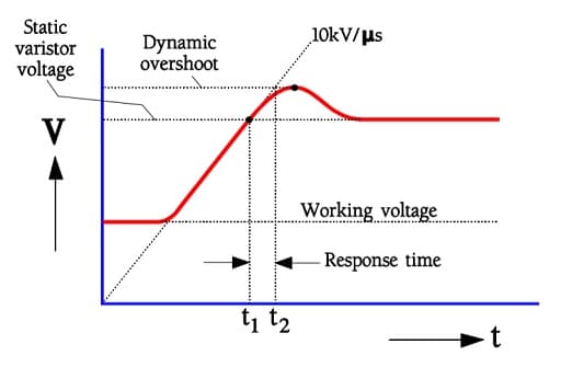
Figure 20. Response time t2-t1 of a varistor.
Varistor Response Time
When a varistor is struck by a voltage transient, the voltage rises across the component until the cutting characteristics start. There is, however, a short delay, a dynamic effect, that produces a certain overshoot, according to Figure 20. For example, an incoming pulse with a rise time of 10 kV/µs is shown. The response of the varistor time is specified as the rise time t2 – t1 in the figure. The response time seldom exceeds 20 ns; multilayer varistor SMDs’ response time is usually less than one ns. The response time sometimes is called turn-on time.
Choice of Type
Choosing the correct varistor presupposes a thorough determination of working voltage, including tolerances, expected transients, their duration, pulse energy and repetition frequency. In addition, we must consider environmental requirements and mounting conditions. Connecting two varistors in parallel to increase the current load capacity should be done only if the varistor voltages (at one mA) differ by less than 1 %. Otherwise, the unbalance of the load may be considerable and, in the most unfortunate cases, amounts to 1000:1.
Failure Modes
The most common failure mode is short-circuiting, which may occur after unacceptably high and energy-rich voltage pulses or after operation at a steady-state voltage beyond the voltage rating. In the latter case, the failure mode might change into open-circuit due to melting effects in the terminal joints or rupture of the package when the large amount of energy generated causes expulsion of the packaging material.
Reliability
The reliability of non-linear resistors, including varistors, is today regarded as relatively good. It depends on serious manufacturers using SPC-based production programs and having verified type approvals. Examples of climatic category classified products 40/125/56 indicate good quality. Furthermore, the rate will be even better if we choose glass/metal packages.
Nuclear radiation
Tests with radioactive radiation in the form of the neutron, β and γ radiation show that varistors can withstand high intensities without any effects on the characteristics.
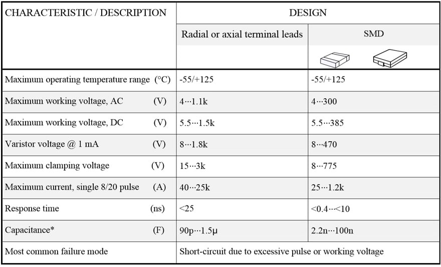
Table 2. VARISTORS CHARACTERISTICS
* Occurring capacitance leads to a capacitive shunting that makes the varistor unusable at higher frequencies.
Applications
Multilayer SMD varistors are used mostly to protect electronic devices from electrostatic discharge (ESD). See Figure 21. and 22. below
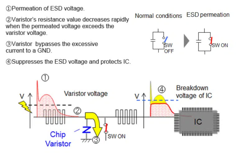
Figure 21. Varistor ESD suppression principle; source: Panasonic
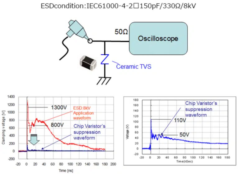
Figure 22. Varistor ESD suppression effect; source: Panasonic
ESD protection benchmarking
Varistor ESD protection applications versus other ESD suppression devices – see Figure 23.
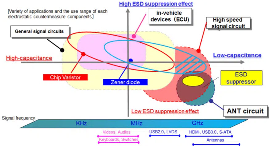
Figure 23. Varistor and other ESD suppression devices application field vs frequency; source: Panasonic
Memristors
Memristors are non-volatile electrically-adjustable resistors. Made mostly from metal oxides, they scale well and are proposed as memory elements in nanometre-scale logic for future brain-like networks.
It was described and named in 1971 by Leon Chua, completing a theoretical quartet of fundamental electrical components which comprises also the resistor, capacitor and inductor. (Figure 25. source: Wikipedia)
Electrical Symbol – see Figure 24.

Figure 24. memristor electrical symbol
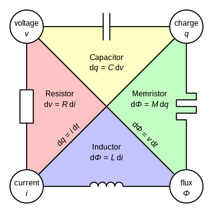
Figure 25. Conceptual symmetries of resistor, capacitor, inductor, and memristor. source: Wikipedia
Memristors have not been yet developed into a mass volume component, nevertheless memristors have gathered a lot of interest by university research as a next generation memory technology by being smaller, more power efficient and yet being able to support more memory states when compared to existing technologies used in our smartphones and computers.
Brain like computing systems using memristors have already been demonstrated.
Detail description is beyond this article scope, for those interested, here are some reference links
- Memristors Key To Nano-Scale Analogue/Digital Adaptive Hardware
- New Memristor Boosts Accuracy And Efficiency For Neural Networks On An Atomic Scale
- Toward Brain-Like Computing: New Memristor Better Mimics Synapses
- First Programmable Memristor Computer Aims To Bring AI Processing Down From The Cloud
- https://passive-components.eu/memristors-supports-brain-like-computing-system/
- Memristors Support Brain-Like Computing System
- Nanometers-Thin Niobium Oxide (NbO2) Memristor Can Bring Breakthrough To Neuromorphic AI Hardware Designs
- Graphene-Based Memristors Show Promise For Brain-Based Computing
Resource: EPCI Blog
A team of experts that brings you the latest and most important news about the EEE Part and Space market.
- Space-Grade components available for immediate delivery - April 10, 2025
- Exclusive stock on doEEEt: How to access and request - April 10, 2025
- Managing EEE components for LEO and lower cost space missions - December 17, 2024
0 comments on Non-Linear Resistors: Thermistors, Varistors, Memristors