Impact of a Decoupling Capacitor in a CMOS Inverter Circuit
- Posted by doEEEt Media Group
- On September 9, 2020
- 0
CMOS Inverter Switching
Let’s start our discussion with a CMOS inverter logic gate in a totem-pole configuration, shown in Figure 1 [1].
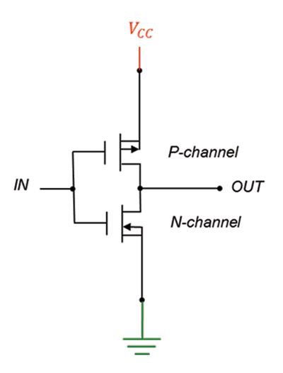
Figure 1: CMOS Inverter Logic Gate
In high-speed digital circuits, one often encounters the cascaded CMOS configuration shown in Figure 2a. A simplified model of this configuration is shown in Figure 2b.
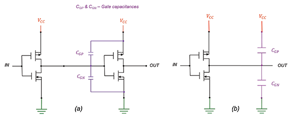
Figure 2: a) Cascaded CMOS configuration, b) simplified model
Let’s investigate the operation of this configuration on the low-to-high and high-to-low transition of the input to the first inverter.
First, assume that the load capacitors CGP and CGN are initially uncharged. When the input signal IN = Low, the upper transistor is ON and the lower is OFF. The current flows through the upper transistor, signal trace, and the capacitor CGN to ground. This is shown in Figure 3a.
Eventually, the capacitor CGN is charged to (approximately) VCC and the current flow stops, as shown in Figure 3b.
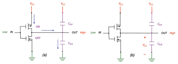
Figure 3: a) Input Signal is Low, b) Current flow stops when CGN is charged to VCC
Now, the driver inverter transitions from low-to-high. Subsequently, the upper transistor turns OFF and the lower transistor turns ON, as shown in Figure 4a.
At this point we have two sources of current:
- Current supplied by CGN as it discharges (dashed arrow).
- Current supplied by VCC as it charges the upper load capacitor.
The current then flows along the trace towards the driver and through the lower transistor to ground. Eventually, the current flow stops and the voltage across capacitor CGP is VCC. This is shown in Figure 4b.
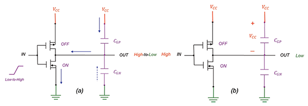
Figure 4: a) Transition from low-to-high, b) Current flow stops when CGP is charged to VCC
Now, the driver inverter transitions from high-to-low. Subsequently, the upper transistor turns ON and the lower transistor turns OFF, as shown in Figure 5.
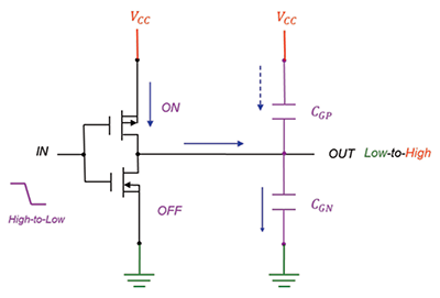
Figure 5: Transition from high-to-low
At this point we have two sources of current:
- Current supplied by CGP as it discharges (dashed arrow).
- Current supplied by VCC flowing through the upper transistor, along the trace, and through the lower load capacitor, eventually charging it to VCC.
Decoupling Capacitor
Now let’s turn our attention to a typical scenario in digital logic circuits with a dc voltage source CMOS driver and a load IC, as shown in Figure 6.
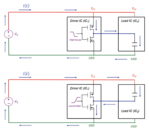
Figure 6: CMOS transistors in a high-speed logic circuit
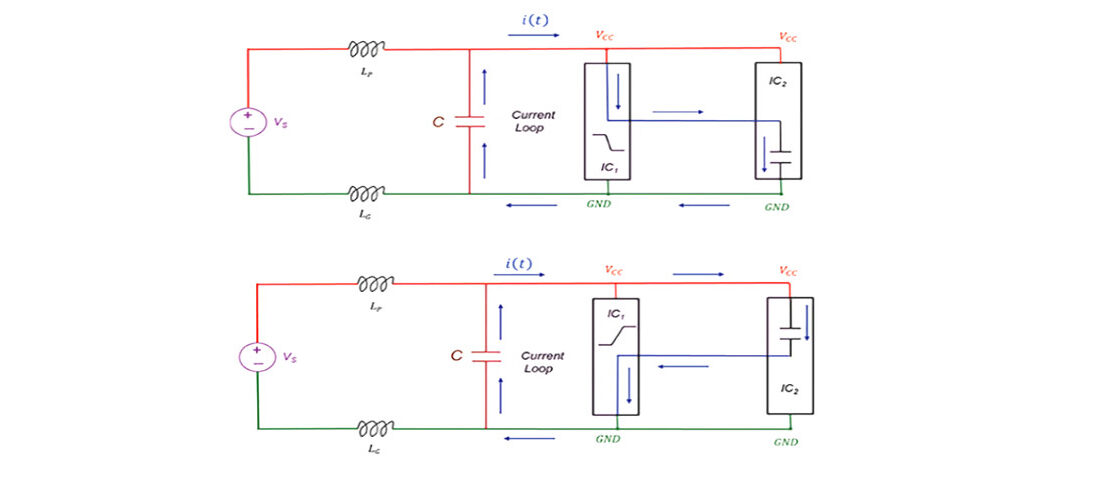
When a CMOS gate switches a current transient is drawn from the power distribution system (PDN). This current flows from the source to the load along the forward path i.e., the power traces and back to the source through the return path i.e., the ground traces.
This time-varying current creates a time-varying magnetic flux that crosses the loop area of the circuit inducing a voltage drop along the traces. We can model this phenomenon by inserting either a voltage source somewhere in the loop, or by inserting an inductance somewhere in the loop. Both the induced voltage and the inductance are distributed along the loop. When the loop is electrically small at the frequencies considered we can model these distributed effects as lumped sources or inductances.
In any practical circuit the forward and return paths (horizontal lines in Figure 9, are orders of magnitude longer than the length of a path between the power and ground pins (vertical lines in Figure 9. It is, therefore, reasonable to insert the lumped parameters only into the forward and return paths. To model the flux-induced effect we will insert inductances along the power and ground traces. This is shown in Figure 7.
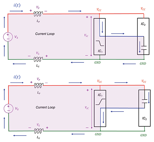
Figure 7: Current loop area and partial inductances
This model applies at lower frequencies where the partial inductances of the power and ground traces connecting the ICs themselves can be neglected. At higher frequencies we would augment the model with additional partial and parasitic inductances between the ICs and within the ICs themselves (see [2] for more details).
When the driver IC switches, the current is drawn from the source resulting in the voltages VP and VG across the power and ground inductances. We often refer to these voltages as a power rail collapse and a ground bounce, respectively.
During the off-switching time (dc condition) inductances act as short circuits and the voltage VIC between the driver-IC power and ground pins equals the source voltage VS. During the switching time the voltage VIC no longer equals the source voltage VS potentially causing signal integrity issues. This voltage now equals
 (1)
(1)
Additionally, the transient current flows in a large loop creating an efficient loop antenna.
Now, let’s place a capacitor between the power and ground pins near the switching IC, as shown in Figure 8.
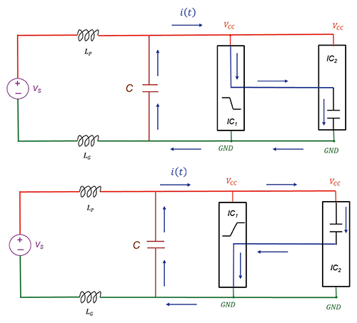
Figure 8: Decoupling capacitor placed near the switching IC
During the off-switching time this capacitor charges to the source voltage VS. During the switching time this capacitor ideally supplies the total required current to the load, as shown in Figure 8.
In reality, it supplies most of the current to the load, thus reducing the current draw from the source and consequently reducing the voltage drops across the inductances. Assuming the ideal scenario, the transient current flows now in a smaller loop, as shown in Figure 9. This, in turn, reduces radiated emissions.
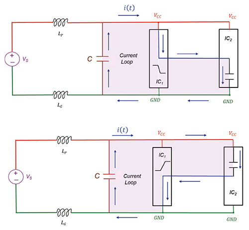
Figure 9: Current loop area with a decoupling capacitor
Decoupling Capacitor Impact – Measurements
The measurement setup is shown in Figure 10.
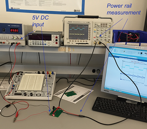
Figure 10: Measurement set-up
The circuit schematic is shown in Figure 11, while the board details are shown in Figure 12.
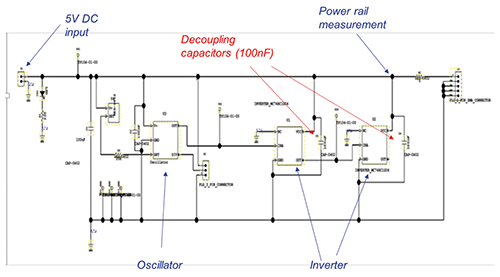
Figure 11: Circuit schematic
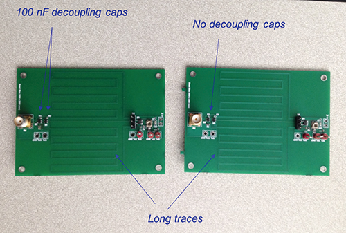
Figure 12: CMOS Inverter board
The board was purposely designed with the very long traces to show the negative impact of the associated inductance, while at the same time increasing the impact of a decoupling capacitor. Figure 13 shows the voltage measurement at the VCC pin of the inverter with no decoupling capacitors.
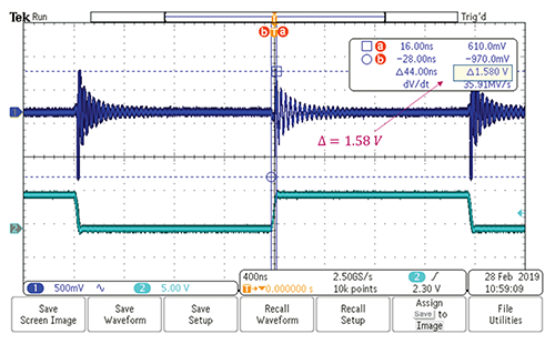
Figure 13: Voltage at the VCC pin at the inverter – no decoupling caps
Notice the peak-to-peak voltage fluctuations of 1.58 V. Figure 14 shows the voltage measurement at the VCC pin of the inverter with the decoupling capacitors.
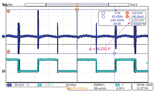
Figure 14: Voltage at the VCC pin at the inverter with decoupling caps
Note the dramatic decrease in the voltage fluctuations from 1.52 V to 232 mV. Finally, Figure 15 shows the radiation measurements with and without the decoupling capacitors.
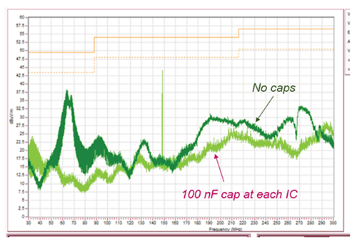
Figure 15: Radiated emissions measurements
Source: InCompliance article
by Bogdan Adamczyk.
References
Bogdan Adamczyk, Foundations of Electromagnetic Compatibility with Practical Applications, Wiley, 2017.
Hubing, Drewniak, Van Doren & Hockanson – Power Bus Decoupling on Multilayer Printed Circuit Boards, IEEE Trans. on EMC, vol. 37, No. 2,
May 1995
Dr. Bogdan Adamczyk is professor and director of the EMC Center at Grand Valley State University (http://www.gvsu.edu/emccenter) where he develops EMC educational material and teaches EMC certificate courses for industry. He is an iNARTE certified EMC Master Design Engineer. Prof. Adamczyk is the author of the textbook “Foundations of Electromagnetic Compatibility with Practical Applications” (Wiley, 2017). He can be reached at adamczyb@gvsu.edu.
- Space-Grade components available for immediate delivery - April 10, 2025
- Exclusive stock on doEEEt: How to access and request - April 10, 2025
- Managing EEE components for LEO and lower cost space missions - December 17, 2024


0 comments on Impact of a Decoupling Capacitor in a CMOS Inverter Circuit