IGBT Snubber Capacitors Selection Guide
- Posted by doEEEt Media Group
- On March 26, 2021
- 0
Important developments of IGBT’s (Insulated Gate Bipolar Transistors) over the years have been focused on increasing power handling capability and increasing reliability. Snubber capacitors have also undergone changes in construction enabling increased power handling capability. This ‘charge’ focuses on giving the reader a brief overview on the IGBT Snubber capacitor.
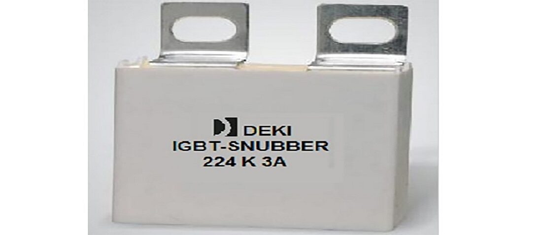
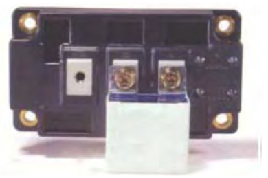
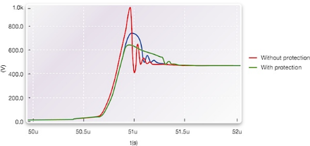
Power systems containing IGBTs must be designed so the transient voltage caused by the high dI/dt that occurs at gate turn off is minimized. Left uncontrolled, this transient voltage can exceed the blocking voltage rating of the IGBT and cause it to fail. In order to minimize the transient voltage a wound construction polypropylene film capacitor mounted as close to the IGBT terminals as possible is usually recommended. (See picture below; credit: Deki Electronics)
The acceptable amount of overshoot voltage is determined by the maximum DC voltage that an inverter power circuit is subject to and the IGBT voltage ratings. The peak current to turn off under a fault condition can be as high as 6-10 times the device current rating. This peak current under the fault condition will proportionally increase the overshoot voltage.
The switching capacity with shortest switching times which can be realized using IGBTs makes it necessary to use an extremely low-inductance circuit design. Even the low self-inductance of the power bus may induce dangerous voltage overshoots between collector and emitter which may result in the destruction of the valuable power semiconductors.
Necessity of Using the Snubber Circuit
These are placed across the various switching devices like transistors, thyristors, etc. Switching from ON to OFF state results the impedance of the device suddenly changes to the high value. But this allows a small current to flow through the switching device. This induces a large voltage across the device. If this current reduced at a faster rate more is the induced voltage across the device and also if the switching device is not capable of withstanding this voltage the device may burn out. So auxiliary path is needed to prevent this high induced voltage.
Similarly, when the transition is from OFF to ON state, due to uneven distribution of the current through the area of the switch overheating will takes place and eventually it will be burned. Here also snubber is necessary to reduce the current at starting by making an alternate path.
Snubbers in switching mode provides one or more of the following functions:
- Shape the load line of a bipolar switching transistor to keep it in its safe operating area.
- Reducing the transient voltages and currents during turn-ON and turn-OFF conditions.
- Removes transient energy from a switching device and dissipate the energy in a resistor to reduce junction temperature.
- Limiting the rate of change of voltage and currents during the transients.
- Reduce ringing to limit the peak voltage on a switching device and lowering their frequency.
Snubber Capacitor Selection Guide:
- Space-Grade components available for immediate delivery - April 10, 2025
- Exclusive stock on doEEEt: How to access and request - April 10, 2025
- Managing EEE components for LEO and lower cost space missions - December 17, 2024


0 comments on IGBT Snubber Capacitors Selection Guide