C-SAM Ultrasonic Analysis to Identify High Voltage MLCC Defects
- Posted by doEEEt Media Group
- On October 19, 2023
- 0
High-voltage multi-layer ceramic chip capacitors (MLCCs) can experience field failures that are instantaneous and catastrophic. The initiator of the loss is often an air gap between an electrode layer and a dielectric layer or within a dielectric layer. The opening may have an X-Y area of any size and may be relatively thick or thin as a micron fraction. They were written by Tom Adams, consultant for Nordson SONOSCAN Inc.
Repeated thermal cycling can cause an air gap to generate a crack extending into the dielectric layer adjacent to the hole. With further thermal cycling, the damage will lengthen and often expand into several crack defects. When damage reaches the next electrode, a conductive or leakage pathway has been formed between two electrodes. The high voltage typically causes the MLCC not merely to fail but to explode — with undesirable consequences. The exact failure mechanism causes lower-power MLCCs to fail but without as much force.
Since high-voltage capacitors consist primarily of many alternating layers of electrode and dielectric, there are many locations where gaps can occur. In any life- or mission-critical application, excluding high-voltage MLCCs having such defects from usage is essential. Thin holes — a tiny fraction of a micron in size — can be just as dangerous as thicker ones.
Gaps of any thickness can be imaged by ultrasound test and measurement, which can distinguish between two solid materials bonded to each other and produce partial reflection and near-total reflection from two solid materials that are in contact but not bonded. When a pulse of ultrasound encounters a gap of any thickness, the solid-to-air interface reflects all of the vibrations to the ultrasonic transducer for collection. None of the pulses crosses the gap because ultrasound at imaging frequencies doesn’t travel through the air.
MLCCs have far more material layers and material interfaces than there are in an integrated circuit package, an isolated gate bipolar transistor (IGBT), or a flip chip, yet the ultrasonic pulse can travel through the whole thickness of an MLCC; it can have dozens or even hundreds of layers, be reflected from the bottom-most interface, and sail back to the transducer with an image to deliver.
This is possible because the electrode and dielectric, although very different electrically, are very close in their acoustic impedance properties. When a pulse strikes the electrode-dielectric interface, there is only a tiny reflection. The remaining pulse is thus free to continue travelling through scores or hundreds of layers in search of a gap, where the solid-to-air interface will reflect it by nearly 100 per cent.
The acoustic images illustrating this article were C-SAM acoustic micro imaging tools in the Nordson SONOSCAN laboratories in Elk Grove Village, Ill. The tool’s transducer travels at high speed while scanning samples. It performs several thousand pulse-echo sequences per second, each at a defined X-Y location. If the pulse encounters only electrode-to-dielectric interfaces, it produces no distinct significant echoes, and the pixel for that location will be black. If it meets a solid-to-air interface, the pixel will be bright white or selected pseudo colour, usually red.
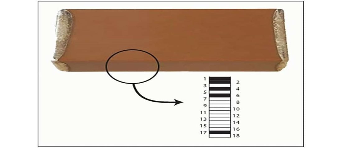
Echoes from interfaces near the top of the MLCC arrive at the transducer first, while those from near the bottom arrive last. For the MLCC shown here, the whole period during which echoes might come from a pulse was divided into 18 parts so each echo could be imaged in its assigned gate. Viewed in sequence, the gate images will show the internal features and the respective depths of those features. Scanning 18 gates, or even more, takes the same time as watching one gate but produces several images.
He MLCC image was 1.8 centimetres long, 7.6 millimetres wide, and 3.8 millimetres thick. Each of the 18 gates is thus about 210 microns thick and is probably several times denser than individual dielectric or electrode layers. The C-SAM tool performed imaging at a frequency of 30 MHz. Most gates did not reveal any defects. The four gates whose acoustic images are shown here are highlighted in the featured image Figure 1. above.
Gate 1 is shown in Figure 1 left. In any sample, Gate 1 conventionally begins just below the top surface but does not include the top surface, which would show only the echoes from the interface between the optically visible surface and the water couplant.
A few minor features are visible in Figure 1. Each is surrounded by a sort of halo (arrow). The halos suggest that these are features such as irregularities on the capacitor’s surface, not internal features. They lie outside the gate but are being imaged as acoustic shadows by ultrasound returning from below. The much larger indistinct dark grey features are acoustic shadows caused by variations in the flatness of the part’s surface. There are no significant internal features within Gate 1 itself.
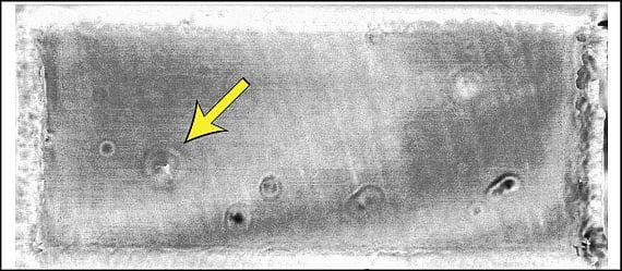
Figure 1 C-SAM image of defective MLCC – Gate 1
In Gate 2 (Figure 2 right), there are a few circular features of various diameters. The shape suggests that they are spherical or pancake-shaped air-filled voids and lie mostly or entirely within Gate 2. Gap-type features such as these can generate the cracks that cause, for example, a communications system to fail. Less distinct circular features may lie partly within Gate 3.
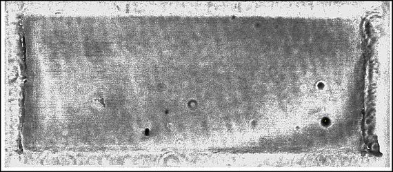
Figure 2. C-SAM image of defective MLCC – Gate 2
In Gate 3 (not shown), no new features were visible. The two features in Figure 1 were visible in Gate 3 as smaller but still bright white versions of their images in Gate 2. It seems likely that these are voids and that they extend vertically through several electrode and dielectric layers. They may have already created conductive pathways that would result in immediate electrical failure when power is applied. It is possible, though, for air bubbles trapped between the green ceramic layers before firing to simply push layers upward and downward without immediately breaching any layer. However, the performance longevity of such stressed structures during active use could be very uncertain.
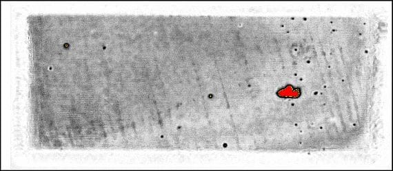
Figure 3. C-SAM image of defective MLCC – Gate 4
The larger void also appears in Gate 6 (Figure 4 right), the result of mild overlap between adjacent gates. Also present is a somewhat unusual feature: the elongated structure marked by the arrow. This is very likely a fibrous dust particle, or more precisely, the fossil of a dust particle that somehow found its way into the green material and was incinerated during firing, leaving behind an empty record of its shape.
There are almost no features of interest below Gate 6, but a feature of interest is imaged by the echoes from Gates 17 and 18. Gate 17, the sharper of the two, is shown in Figure 6 left. The dark feature right of center is the acoustic shadow of the large void in Gates 4 and 5 above. It formed in this way: Ultrasound pulsed by the transducer was locally blocked by the void in Gate 4 and did not reach the bottom of the capacitor. Ultrasound was reflected from all other areas of the bottom but not from the area of the acoustic shadow. The lack of echo signals created an acoustic shadow when reaching the transducer.
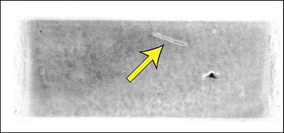
Figure 4. C-SAM image of defective MLCC – Gate 6
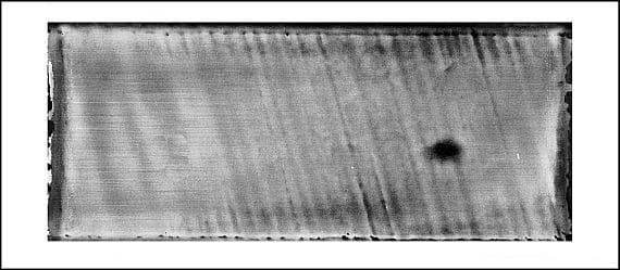
Figure 5. C-SAM image of defective MLCC – Gate 17
- Managing EEE components for LEO and lower cost space missions - December 17, 2024
- Filtering Characteristics of Parallel-Connected Fixed Capacitors in LCC-HVDC - November 21, 2024
- ALTER SPACE TEST CENTER: testing approaches for New Space - September 30, 2024

0 comments on C-SAM Ultrasonic Analysis to Identify High Voltage MLCC Defects