RC Snubber Design for SMPS Protection (Part I)
- Posted by doEEEt Media Group
- On May 13, 2019
- 0
Fundamentals of Inductive Switching and RC Snubber Impact
This is the first of the two articles devoted to the topic of an RC snubber design. In Part I, we discuss the fundamentals of inductive switching and the need for circuit protection. The impact of an RC snubber on the circuit performance is demonstrated through a series of simulations. Part II (to appear in the March 2019 issue of In Compliance) will address the systematic process of the snubber circuit design, together with the simulation and verification through the laboratory measurements.
Switching in an Unprotected Inductive Circuit
Consider the circuit is shown in Figure 1(a). When the switch is closed, in steady-state the voltage across the inductor, vL, is zero, and a dc current I0 flows through the inductor. The energy stored in the magnetic field of the inductor is
When the switch opens, a large negative voltage develops across the inductor and subsequently the switch. The magnetic energy stored in the inductor is dissipated in the arc across the switch contacts or is radiated, as shown in Figure 1(b).
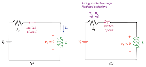
Figure 1: Inductive circuit – a) switch closed, b) switch opens
This behavior is often destructive to the switch and some sort of a protective circuitry is required. Before introducing a possible solution (RC snubber) let’s augment the circuit of Figure 1 with the stray capacitance of the wiring, as shown in Figure 2.
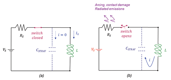
Figure 2: Inductive circuit with a stray capacitance – a) switch closed, b) switch opens
When the switch is closed, in steady-state no current flows through this capacitance. When the switch opens, the inductor’s current now flows through the stray capacitor charging it, and the voltage across it rises at an initial rate of . When this voltage exceeds contact breakdown voltage, an arc occurs across the switch contacts [1], and the capacitor discharges. When the arcing stops the current charges the capacitor again potentially causing another arcing.
The electrical oscillations occurring in this LC resonant circuit when the switch is opened are often the source of the voltage transients and high-frequency emissions. The voltage and current transients often manifest themselves as the ringing waveforms, like the one shown in Figure 3 [2].
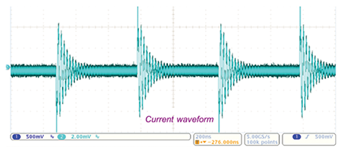
Figure 3: Current ringing waveform
These oscillations can be reduced by placing a snubber across the switch, as shown in Figure 4.
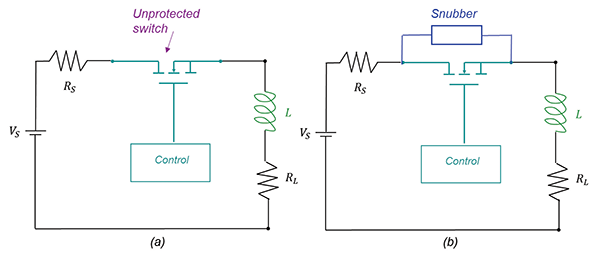
Figure 4: Circuit with an inductive load – a) switch unprotected, b) switch protected with a snubber
There are many different kinds of snubbers; this paper focuses on the most widely used – an RC snubber. The RC snubber design discussed here is used in a step-down or buck SMPS.
A typical buck SMPS schematic with an RC snubber across the low-side FET is shown in Figure 5.
A typical buck SMPS schematic with an RC snubber across the low-side FET is shown in Figure 5.
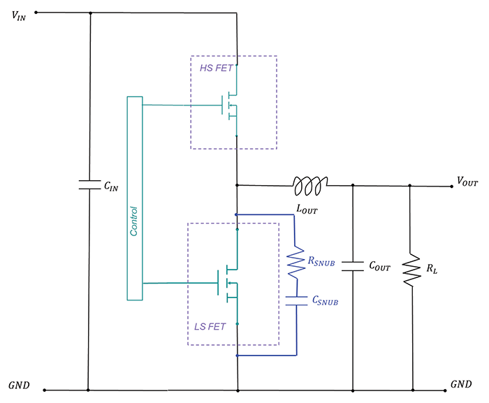
Figure 5: Typical buck SMPS schematic with a snubber across the lower FET
Figure 6 shows the same buck SMPS with the parasitic capacitances and inductances explicitly shown [3].
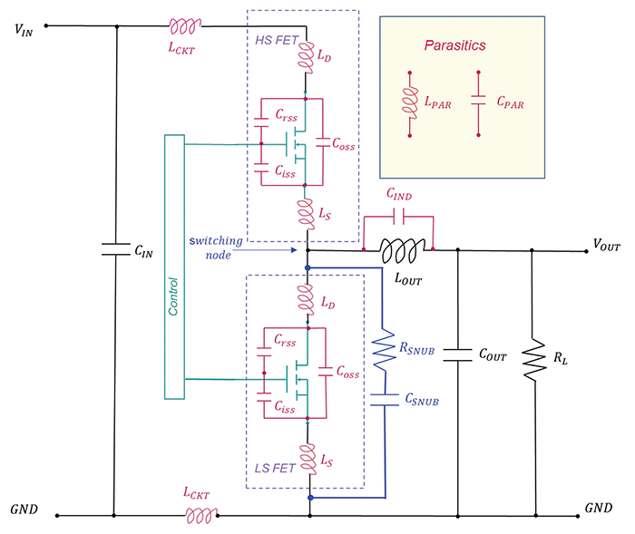
Figure 6: Typical buck SMPS schematic with parasitics shown
The impulse voltage generated at the switching node stimulates the parasitic components to resonate as a damped LC network. The purpose of the RC snubber placed across the low-side switch is to reduce these oscillations to an acceptable level.
RC Snubber Impact
The basic resonance frequency in an RLC network is [4],
The resonant frequency in a circuit shown in Figure 6, without a snubber in place, is
A simple circuit demonstrating this behavior is shown in Figure 7.
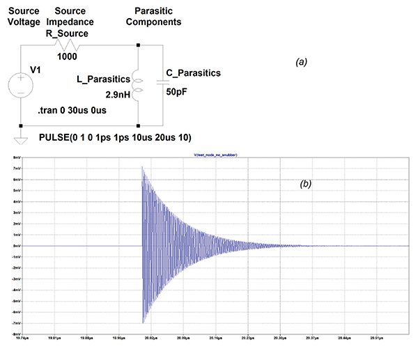
Figure 7: LC parasitic circuit without a snubber: (a) schematic, (b) voltage at the switching node
A close-up of the ringing waveform shown in Figure 8, reveals the ringing frequency of 412.9 MHz.
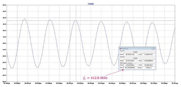
Figure 8: Ringing waveform and its frequency (no snubber)
FFT of the ringing waveform is shown in Figure 9.
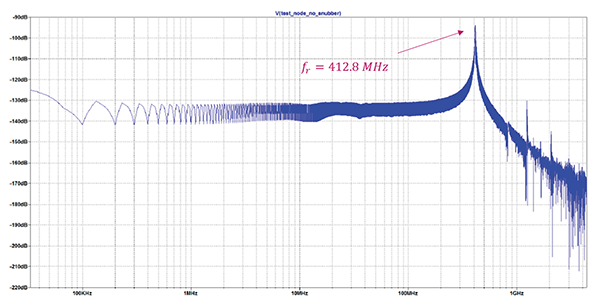
Figure 9: FFT of the ringing waveform (no snubber)
To move the resonant frequency to a lower value a 150 pF capacitor is added between the switching node and reference, as shown in Figure 10.
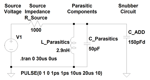
Figure 10: LC parasitic circuit with a 150pF capacitor added
The resulting ringing waveform is shown in Figure 11.
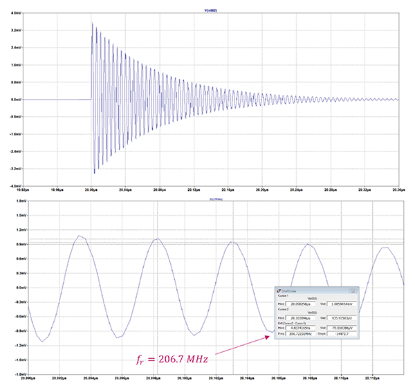
Figure 11: Ringing waveform with a 150pF capacitor added
Note that the ringing frequency has been reduced from 412.8 MHz to 206.7 MHz.
Using a capacitor-only snubber is generally not recommended [1]; to limit the discharge current of the snubber capacitor (and protect the switch) a resistor if often placed in series with the capacitor.
Figure 12 shows a full RC snubber circuit, with a 7.5 Ω resistor added.
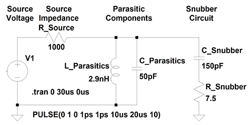
Figure 12: LC parasitic circuit with a snubber
The resulting ringing waveforms are shown in Figure 13.
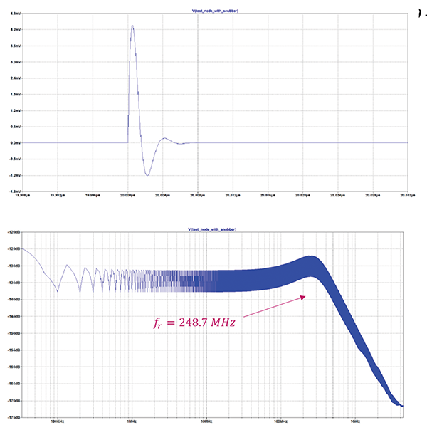
Figure 13: Ringing waveforms with a snubber added: (a) close-up of a time domain waveform, (b) FFT of the waveform
Note that the resonant frequency increased from the capacitive snubber value in Figure 11 but is still much lower than that of the un-snubbed circuit.
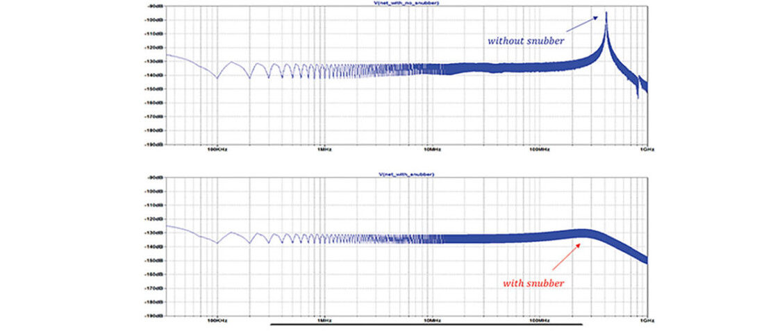
Figures 14 and 15 clearly show the dramatic improvement of the RC-snubbed circuit response compared to the un-snubbed one.
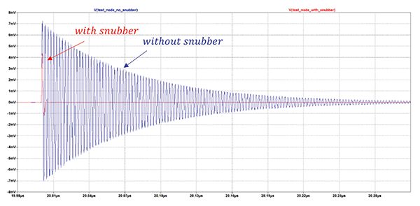
Figure 14: Comparison of the circuit responses: time domain waveforms with and without snubber
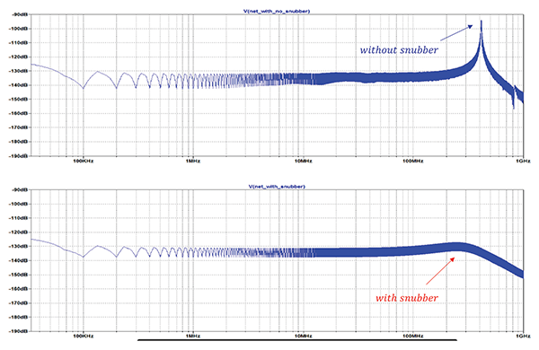
Figure 15: Comparison of the circuit responses: FFT of the waveforms with and without snubber
Source: InComplianceMag article
by Bogdan Adamczyk and Bill Spence.
- Space-Grade components available for immediate delivery - April 10, 2025
- Exclusive stock on doEEEt: How to access and request - April 10, 2025
- Managing EEE components for LEO and lower cost space missions - December 17, 2024




0 comments on RC Snubber Design for SMPS Protection (Part I)