Power Output Optimization in Switching Regulator
- Posted by doEEEt Media Group
- On December 9, 2020
- 0
Existing test solutions aren’t always suitable for the latest improvements in switching regulator technology. Transient load testing can address these inequities.
As electronic system loads (integrated circuits, electromechanical devices, etc.) increase in current level and complexity, it places greater demands on voltage sources to provide adequate current supply and voltage regulation. Historically, a common practice among engineers has been to lean on capacitors to ensure adequate power-supply bulk decoupling. In turn, adequate testing of these regulators requires an equal increase in testing sophistication.
Step transition rate needs to be significantly faster than the voltage regulator control loop to adequately exercise the converter. Since various converters have different loop bandwidths, how fast is fast enough? In terms of current slew rate, fast enough also depends on the size of the load step.
For example, consider a load step of 2 A with a slew rate of 2 A/μs. The total transition time is 1 μs, which we will equate to rise time (10% to 90%). Rise time is approximately 2.2 times the circuit time constant τ, which equals 1/(2πf). In this example, f calculates to 350 kHz, which is significantly faster than most loops, so this load step can provide useful information.
However, if the load step is 120 A with the same slew rate of 2 A/μs, then transition time is 60 μs, which correlates to a frequency of only 5.8 kHz. That is dismally slow for exercising a high-performance voltage regulator! Rather, we would want a slew rate of at least 120 A/μs, or even faster for the fastest multiphase regulators up to about 1200 A/μs.
With small local load slammers, maximum slew rate will be limited by board and connector parasitics, so as they say, your mileage may vary. But it will still be orders of magnitude better than an external load unit.
Beyond that, there’s the issue of accurately measuring a current transition that fast. Current probe loops introduce far too much inductance to allow fast transients, and even chip resistors for current sensing must be compensated for their internal inductance. We will leave that topic as outside of the scope of this article.
Controllable transition rate is necessary, as discussed above, for different load step magnitudes to achieve a desired overall transition speed. Not all loads require a high slew rate, so adjusting it can be employed to match varying di/dt requirements of the actual load. If fast enough, it can help debug the system decoupling solution.
Controllable step frequency and duty cycle help tailor the test to a particular converter. For example, a very fast loop may recover quickly enough that a slow repetition rate yields little information other than a very brief recovery time. On the other hand, a slow loop simply won’t respond to fast step frequencies. It yields information about the output decoupling, but little about the converter loop.
Arbitrary load profile capability allows a load to vary in a nonlinear manner over time. It can be used to imitate startup and state change currents, or specific functions (read/write, processor operations, electromechanical loads).
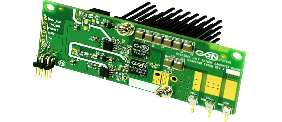
A low impedance connection to the circuit board is required for best performance. Since there’s typically not room for mounting the slammer on the board, a multi-pin, low-inductance connector should be placed appropriately to allow it to plug in directly. Once system operation is verified, subsequent board builds may remove the connector footprint or simply not install it. Alternatively, a slammer could be directly soldered to the board with a short copper strip near the decoupling capacitors.
Adequate dissipation capability is desirable for DC testing, as well as thermal testing. This is a challenge for small load slammer units due to their size. Some are better than others, but it may be necessary to use a larger external load unit or resistor bank for this testing.
Protection circuitry is a second area where slammers bow to larger external load units. They typically are less robust in terms of overvoltage shutdown, reverse-voltage protection, overtemperature, and the like. But do they at least have some protection such as fusing or temperature sensing? Or are they priced low enough that they can be considered disposable?
What instrumentation outputs are available from the load slammer? Does it read DC current and voltage? Transient response voltage? How fast does it update? How accurate is it? Most slammers are not calibrated. Do you need that, or are you okay with an uncalibrated device? Or, does the unit simply have a coaxial connector or other test points for plugging in a scope probe?
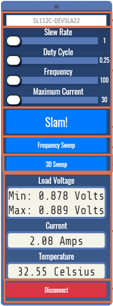
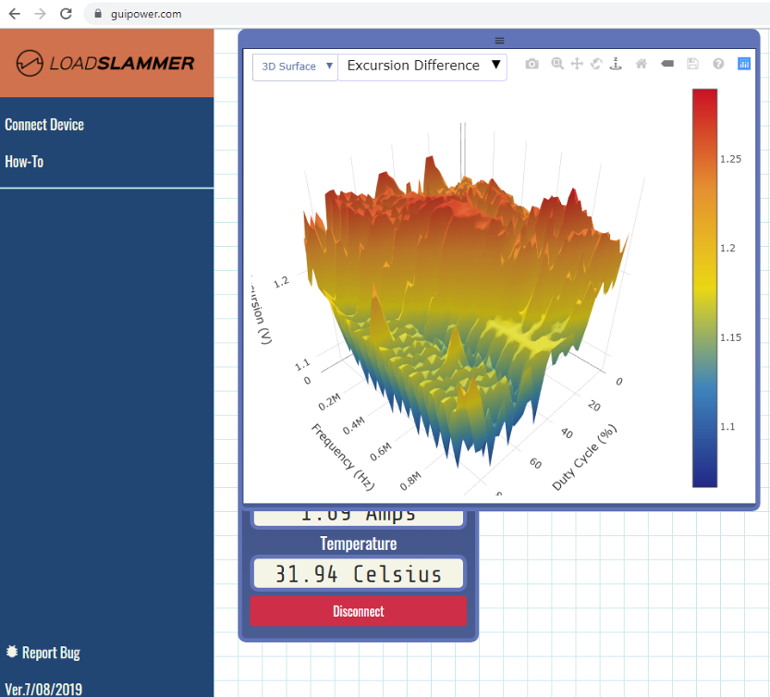
Ease of use is important to get the most out of a load slammer. This speaks mainly to the GUI (Figs. 1 and 2) used to set up and operate the load. Does the software install easily and work properly? Is it buggy? Is it easy to initialize and operate? Can it be integrated into a larger automated system?


2. Features of a LoadSlammer include automated test vector generation and 3DSweep functionality.
In the final analysis, users will balance the features that they need versus those that they would like to have, which brings us to cost.
Cost is always a factor, and not just for limited budgets. If you need the best, you can always buy the best. However, if a less expensive load slammer does what you need for a specific application, it can minimize your investment, freeing more money for other things. You may be able to simply expense it and be up and running, rather than wading through the capital equipment process. That saves time as well as money. It may also allow for purchasing of dedicated units for each lab bench or for each production test fixture.
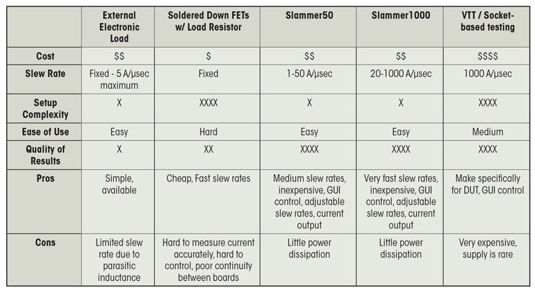
The table compares several of the currently available load slammers.

A Bit of History…
Those of us who have been around for a while have observed how dramatically computers and other electronic systems have changed over time. Computer enclosures went from buildings to cabinets to boxes to boards to ever-shrinking chips. Power systems have followed suit.
Somewhere in the Middle Ages of computing (late 1980s), power systems began a major shift. Starting as multiple boxes of low-voltage outputs with hundreds to thousands of amperes of capacity, they gave way to higher-voltage central sources with board-level distributed regulation. This trend spread to smaller machines. By the early 2000s, desktop computers regulated high-current outputs separately, relying more and more on the 12-V output of their silver box supply rather than 5 V or 3.3 V.
Notebooks carried the concept even further, with a single output brick supply and all-local regulation. Recent notebook generations have further evolved, becoming much like power systems found in smartphones. Multiple board-level voltage regulators and load switches combine to save energy and reduce heat, allowing simultaneous increases in performance and battery life.
Processors and other large ICs follow suit, shutting down unnecessary portions and functions to save heat, allowing bursts of higher performance without overheating. They also do it in concert with the regulators powering them, optimizing voltage as performance and power savings dictate.
So why the history lesson? History is a flow, where the past explains the present and informs future direction. There are four takeaways from this regarding our topic:
- Semiconductor improvements and increased demand management have significantly increased step current requirements over early computing, making greater demands of power sources and output capacitor networks.
- Accordingly, verification of power sources increasingly requires emphasis on response to load transients dictated by power-supply loop bandwidth and capacitance.
- Because both loads and power sources are now distributed on the same board, test loads must be similarly located. External load units with long connections are inadequate for transient testing due to their parasitic inductance.
- The dual trends of decreasing size and increased power management will continue. Power-management techniques will expand in depth and complexity for large ICs and will propagate more to medium and smaller ICs and the discrete components that complete the solutions.
Source: Electronic Design article
- Managing EEE components for LEO and lower cost space missions - December 17, 2024
- Filtering Characteristics of Parallel-Connected Fixed Capacitors in LCC-HVDC - November 21, 2024
- ALTER SPACE TEST CENTER: testing approaches for New Space - September 30, 2024

0 comments on Power Output Optimization in Switching Regulator