Design for manufacturing and assembly
- Posted by Mario Rueda Aguilocho
- On March 30, 2022
- 0
Design for manufacturing is based on design rules from manufacturing processes for both the PCB and Electronics assemblers. Some authors prefer to have separate definitions for the PCB Printed Circuit Boards manufacturing by grouping them under different names DFF, Design for Fabrication and DFA, Design for Assembly for just the electronics assembly process.
In this article, we prefer to use just one term, Design for manufacturing DFM, which includes the complete process from PCB fabrication to the end of the assembly process in the electronics manufacturing facility.
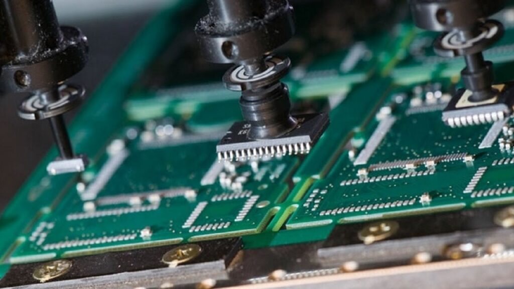
Figure 1: SMD Pick & Place equipment
Design for Manufacturing process
When we speak about electronics product development, design and manufacturing are considered separate processes most of the time. However, these processes should be regarded as a single process with a feedback loop back to the designer. This is how development should be considered to make competitive, fast-to-market, and lowest cost products.
When manufacturing is considered during the design process, progress has already been made toward accelerating new product introduction and optimizing line processes. Design for fabrication, assembly, and test, when considered throughout the design function, helps prevent the manufacturer from drastically changing the design data or sending it back to the designer for redesign.
The Design and Manufacturing process starts with a change in how manufacturing is seen. Design for manufacturing should start at the beginning of the invention, when the design engineer is building the schematics, and continue through the entire design process.
Step 1. Having a library of proven parts
The first Design for Manufacturing step is to have a library of proven parts, both for schematic symbols and component geometries. This forms the basement for quality schematic and physical design.
Then, during schematic design, the Design for Manufacturing DFM process requires communication between the designer and the rest of the engineering teams, including procurement, assembly, and test by providing a bill of materials (BoM). Purchasing team can determine if the parts can be procured in the volumes necessary, timing, and at efficient costs.
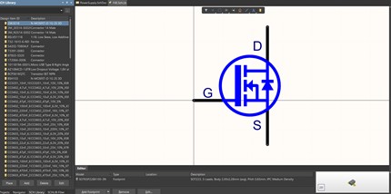
Figure 2: Altium Library Sample
Can the parts be automatically assembled, or would additional costs and time be required for manual operations? Can these parts be tested using the manufacturer’s test equipment? How does the lead time look for these parts? After these reviews, the designer’s feedback can help prevent either a redesign or additional product costs in manufacturing. With today’s market situation, it is important to have a frozen EBOM as soon as possible, so that procurement can start to do its job.
Step 2. Fabrication, assembly, and testing
The next Design for Manufacturing step is to ensure the layout can be fabricated, assembled, and tested.
PCB fabricators do not just take the PCB output data package and go straight to manufacturing. Instead, fabricators always run their checklist macros or SW with fabrication rules against the data to ensure they will produce boards that are not hard failures and determine adjustments to avoid soft failures that could decrease production yields. After this check is done, there are always Engineering Queries between supplier and PCB designer to solve the potential issues.

Figure 3: Electronic circuit
So, for the PCB designer, part of the Design for Manufacturing is to use the same set of rules while doing the PCB layout. By doing this, we can save time by reducing the loops of engineering queries and redesigns required to the layout and generating output data several times.
Other factors to consider are related to the cost, use the via size and track width that will do the job regarding the board functionality. For example, do not use 0.15 mm vias if they are not needed, as these vias are more expensive than 0.3mm ones.
Effective, accurate component placement considers the best practices of design and assembly, both interconnected. The layout engineer must take special care to correctly place components on the board since this directly influences assembly and testability.
Also, with the evolution of various technologies, assembly takes on newer meanings, dimensions, and demands.
For example, fine-pitch BGAs and QFNs are challenging current assembly practices and procedures. PCB design and assembly know-how and experience are key factors for effective placement in these situations.
Step 3. Considering technical and mechanical aspects
Design for Manufacturing considers such factors as through-hole versus surface mount components, critical ribbon and cable assemblies, connector types, cutouts, vias, decoupling capacitor placement, mechanical aspects, and others. Nowadays, through-hole technology is just for special components or technologies (connectors, power electronics…), while the surface mount is the basis for most of today’s designs.
In terms of placement and routing, the beauty of an SMT design is its advantage relative to the board’s area because both sides of a board can be used for components placement. This creates certain challenges, however. For instance, an experienced PCB designer doesn’t want to place a noise-generating device or high–frequency, sensitive device close to the clock where the signal will incur interference. Improper component placement raises the probability of high-level noise and an unacceptable signal-to-noise (SNR) ratio.
Through-hole is mostly used for connectors and is limited to signals coming into and exiting the PCB. However, SMT connectors are increasingly used. But some applications employ a combination of surface mount and PTH components. When a PTH connector is used, another component cannot be placed on the other side of the board since there’s no usable area due to the pins and selective soldering keepouts.
PCB designers must take precautions when placing either PTH or SMT I/O connectors. The same concepts apply to other components with gold fingers, ribbons, or cables attached to the board. Usually, the physical location of these devices is fixed by the mechanical Team as it is connected to other parts in the system outside our PCB. Any component that must keep its location fixed will fall under this category.
At the same time, the board designer must ensure space limitations are not violated, and no mechanical, vibration or height-related issues are created due to that particular placement. The designer also must check that all XY Coordinate Calculations are accurate. Before releasing the fabrication data, physical location and dimension calculations must be checked carefully.
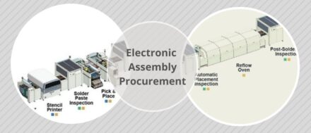
The boards’ assembly process is not just the components pick and place operation, but the complete process including PCB destacker, Solder paste application, paste inspection, pick&place, reflow, AOI, In module programming, Selective soldering, In-Circuit Test, Functional Test, Conformal coating, final assembly, burning, packing… and PCB design must consider all these processes to maximize manufacturing efficiencies.
For instance, proper pad openings will help to decrease solder paste stencil cleaning, balancing heavy components on the board will help to avoid board warpage from the component weight, heavy components on one side will avoid components to fall off during the second pass reflow process, proper silk screen clean up will help AOI to be more efficient, proper test point size will help In module programming, Test points in all nets and proper clearance will make the ICT engineers very happy, keeping appropriate keep out areas from selective soldering pins is a crucial factor in avoiding solder touch-ups later on, etc.
Design for Manufacturing: Repair and troubleshooting process
The design also needs to consider the repair and troubleshooting process; for instance, BGAs should never be placed close to the board’s edge. Reason: A BGA needs a peripheral area that’s heated during rework. If close to the edge, that half side close to the edge will not sufficiently heat, simply because there’s no mass around the BGA device to heat. Hence, the BGA will be complicated to depopulate.
PCB designers should know the impact of the design on all these processes, including board handling (I have seen problems with shape corners on boards causing issues in Manufacturing). It is an excellent recommendation to visit manufacturing plants to see the process and speak to the process technicians and engineers.
Design for Manufacturing techniques needs to be applied from the beginning of a project if we want the project to be successful.
GET IN TOUCH TODAY!
Do you have questions? Contact us!
Related Posts
- Electronic Assembly Procurement - April 1, 2022
- Prototyping Service - March 31, 2022
- Electronic Design: Technical design capabilities - March 31, 2022






0 comments on Design for manufacturing and assembly