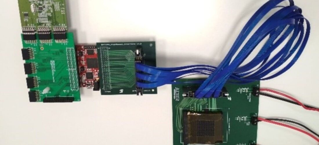
Image Sensors: Characterization according to the EMVA 1288 standard
- Posted by Pawel Adamiec
- On February 15, 2022
- 0
The image sensor is the heart of any digital camera. For many years, digital cameras were essential devices for space exploration used for image acquisition of flyby objects like planets or moons, earth observation, and monitoring the spacecraft’s status. In the last decade, digital cameras invaded the cell phone market allowing everyone to take so loved selfies and document everyone’s life. Recently, they have entered the automotive market as rear cameras to help during car parking, and soon they will be mandatory inside the cabin for driver monitoring.
But how do you choose the best sensor for the camera? The response could be quite easy; take the datasheet and compare! But wait …, the parameters in datasheets are different, even worse …, the units are other for the same parameters. These are the daily dilemmas of camera designers. Therefore, almost 20 years ago, representatives of the European machine vision industry established the European Machine Vision Association (EMVA), which issued an EMVA1288 Standard for Characterization of Image Sensors and Cameras. The sector received the standard well, which finally had a tool allowing comparison between the sensors. Our goal is not to introduce the standard here (however, we encourage the readers to learn more about it) but to show how it was implemented in the ALTER labs.
The EMVA1288 standard lets us measure the crucial parameters of the image sensors and cameras, converting the physical model of the camera (image sensor) to the mathematical model, where the parameters can be extracted (see Figure 1).
Figure 1 (a) Physical model of the camera and (b) Mathematical model of a single pixel. Figures separated by comma represent the mean and variance of a quantity; unknown model parameters are marked in red.
The incident photons from the object undercome some physical processes inside the pixels and camera electronics resulting in a picture we can see on the screen of our beloved cell phone (or other devices). The mathematical model allows obtaining the following parameters, but not limited to responsivity, efficiency, saturation capacity (full well), signal-to-noise ratio (SNR), dynamic range, temporal noise, linearity, and dark current (also its temperature dependence).
Besides, the spatial nonuniformity ie. dark signal nonuniformity (DSNU) and photoresponse nonuniformity (PRNU) together with the defect pixels can be found.
Optical setups
For the measurements according to the standard, a setup with a light source is required that irradiates the image sensor homogenously without a lens with an f-number equal to 8 (see Figure 2). In our setup, we use the integrating sphere together with a set of LEDs or monochromators according to the needs. The LEDs used in the setup are commercially available components in the wavelength range from 405 nm to 1550 nm with FWHM less than 50 nm. In the case of the monochromator, the available range is from 350 nm to 2600 nm using a broadband light source like a tungsten-halogen lamp. In both approaches, the setups allow for the characterization of monochrome, standard RGB image sensor, or any hyperspectral image sensor in the mentioned wavelength range.

Figure 2 Requirements for optical setup for the irradiation of the image sensor by a disk-shaped light source (left) and the scheme of the setup at ALTER labs (right).
According to the EMVA standard, the relative irradiance decrease at the edges of the image sensor should be less than 0.5%.
In our setup, the opening diameter of the integration sphere is about 50 mm. In contrast, the opening where the device under test (DUT) is placed is rectangular with dimensions 45mm x 40 mm, and the image sensors are usually smaller.
The power distribution over the horizontal (black) and vertical (red) DUT position is within the necessary range, as shown in Figure 3 for image sensors with sizes up to 42 mm x 36 mm. On the other hand, when the darkness is necessary to acquire the dark images, our setup allows for -100 dBm or femtowatts power level (background noise of the reference detector), which in principle, can be considered as excellent dark conditions.
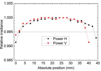
Figure 3 Relative irradiance at the DUT position.
Our setups can be used for characterization at different temperatures through climatic chambers, as shown in Figure 4. The image sensor is placed inside the room and the light source and readout electronics outside the section.
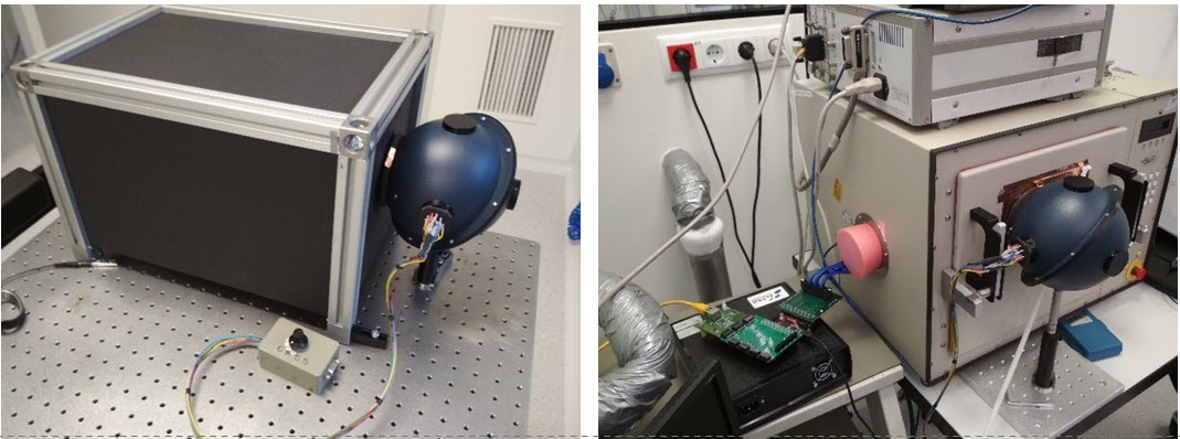
Figure 4 Realize the optical setup for room temperature (left) and high/low-temperature measurements (right).
Test boards and electrical measurements of image sensors
Depending on the client’s needs, the custom camera can be developed, or the evaluation board (camera) delivered by the client can be used. The test board developed in ALTER consists of two parts: (i) motherboard with FPGA memories, SPI, and all necessary electronics to drive the image sensor and (ii) remote board with zero-insertion force socket to hold the image sensor together with accompanying MLCC components. Such a solution allows measuring the image sensors not only at ambient conditions, but for specific customer environments for automotive or space applications ie. thermal chambers, humidity, thermal vacuum, and radiation.
The motherboard is supporting the single-ended and differential signals from the image sensors. The image sensor can be driven by internal power supplies from the motherboard or external high precision power supplies like Keithley 2602B Source Meter. Besides, the power rails of the image sensors can be monitored independently in all mentioned environments. The realization of the test boards is shown in Figure 5.
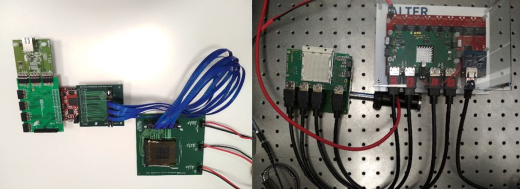
Figure 5 Test boards for the image sensors with single ended signals (left) and differential signals (right).
Examples of the results
According to the standard, we need to acquire at least 2 dark and 2 grays (flat) images at 50 exposure times. The number of exposure times can be reduced to 9 suitably chosen for production purposes. Usually, we are working with tens of image sensors, so the number of exposure times is reduced to 25, especially if the color sensors are tested.
The next viewgraphs show examples of the photon transfer curve, sensitivity, and SNR plot for a commercial 10-bit image sensor. The photon transfer curve allows obtaining overall system gain, whereas sensitivity plots the responsivity, thus leading to the computation of the quantum efficiency. This plot gives us also information about the saturation of the pixel, which is a very important parameter leading to the information about the full well capacity of the image sensor. The SNR graph contains the measured SNR values, the theoretical curve according to the linear camera model using determined parameters, and the SNR curve for the ideal sensor (for a full explanation, please refer to the standard).
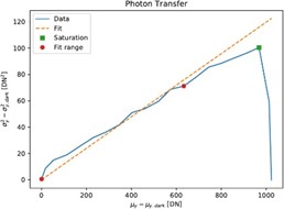
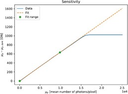
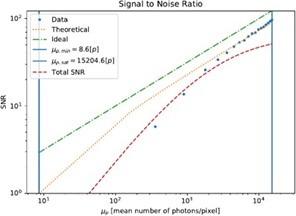
Figure 6 Photon transfer curve, sensitivity plot (previous page), and SNR plot.
A set of images needs to be taken at 50% of the saturation capacity to calculate the spatial properties. Again, the quantity of the acquired images depends on the purpose, i.e., for the production, it is enough to reach 16 dark and 16 gray photos. However, it is better to suppress the temporal noise to such an extent that it no longer influences the spatial noise’s standard deviation, which requires averaging over 100 or more images. Since we are working with higher amounts of image sensors, we are acquiring 16 images usually. The spatial properties are calculated and presented as logarithmic DSNU and PRNU (see Figure 7). It is easy to find the outliers and regions with deviations in these charts’ dark and gray images. It can be seen that most of the pixels of this 1.3 Mpix image sensor are within the normal distribution (model).
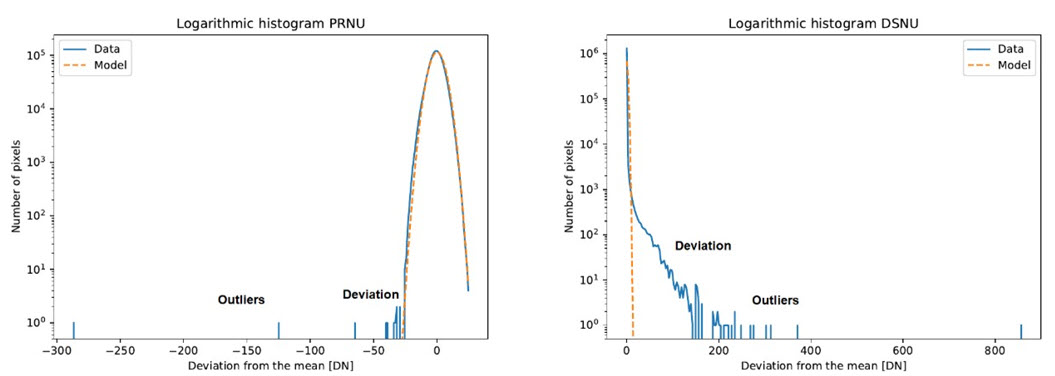
Figure 7 Logarithmic histogram of DSNU and PRNU for 1.3 Mpix image sensor.
Another very important parameter is the dark current. This measurement requires no illumination source, and a high level of darkness is necessary, delivered by our setup. The dark images obtained from the sensitivity measurements can be used to calculate the dark current. However, it might be needed to use much longer exposure times for shallow dark currents. At least six equally spaced exposure times must be chosen for these measurements. Since our setup is prepared for measurements in different environments, Figure 8 (up) shows the measurements of the dark current at -60°C in the climatic chamber for 4 Mpix 8-bit image sensor. From this plot, it can be seen that the image sensor has quite a high offset, that the dark current could not be obtained from the sensitivity measurements due to too short exposure times (red points), and therefore the longer exposure times were used (blue points). Temperature dependence of the dark current for the same sensor is shown on the right-hand side. The image sensor was thermal cycled in the temperature range from -60°C to 60°C, and no hysteresis was found. The y-axis is in the logarithmic scale to see the changes in all measured ranges.
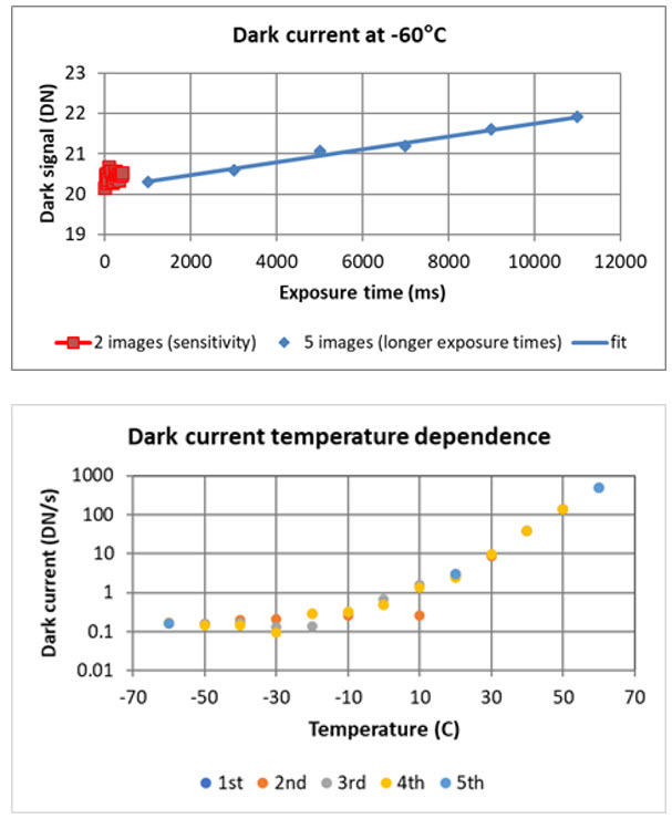
Figure 8 Dark current at -60°C (up) and the dark current dependence on the temperature (down).
We can also monitor the consumption on different power rails of the image sensor. Figure 9 shows the currents at three power rails of the commercial image sensor. The peaks in the digital currents coincide with the image acquisition so the current has elevated from the idle state of 5 mA to the picture acquisition state of about 16 mA.
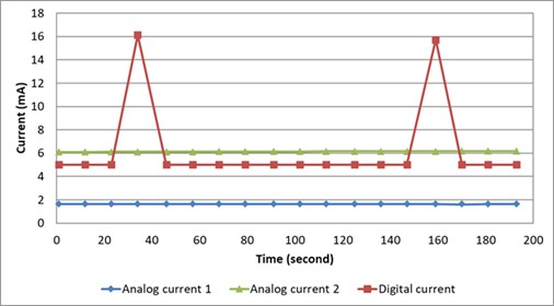
Figure 9 Monitoring of the current consumption on three power rails.
Summary
We have developed an EMVA standard-compliant system for characterizing image sensors in a wide wavelength range and produced a low-cost camera to drive different image sensors. The camera consists of the leading electronics and the remote socket to hold an image sensor, making it a flexible test board for temperature, vacuum, or radiation tests with image sensors for space or automotive applications.
GET IN TOUCH TODAY!
Have questions? Contact us!
- Image Sensors: Characterization according to the EMVA 1288 standard - February 15, 2022
- Development of a NIR-VIS-UV lidar echo emulator - October 7, 2021
- LIDAR echo emulator - October 7, 2021

0 comments on Image Sensors: Characterization according to the EMVA 1288 standard