The behaviour of GaN power HEMTs subjected to short circuit
- Posted by Omar CHIHANI
- On October 26, 2022
- 0
Investigation
Introduction
Gallium Nitride high electron mobility transistors (GaN HEMTs) are becoming very attractive for power applications nowadays. Thanks to its superior intrinsic characteristics, GaN material can operate in high temperatures [1], reduce the size of the components, and operate at high frequencies [2]. These aspects can then allow the weight reduction of the entire system, including passive components and cooling systems.
Different types of GaN power HEMTs are actually present in the market. Among all these types, the enhancement mode (E-mode) transistor is preferred due to its normally off behavior ad the large power range available. However, these kinds of devices can face extreme conditions related to SC in most applications [3], [4]. Therefore, it is essential to understand the behavior and capabilities of these components regarding the SC conditions. This will be a massive input for the design of protection circuits.
This paper takes part in this approach of having a better understanding of the e-mode GaN HEMTS behavior regarding SC operations in order to point out the critical elements leading to the failure of such components.
Component and Test setup
The component used for the investigation is a commercial 650V E-mode GaN exhibiting a maximum continuous drain current of 60A at 25°C.
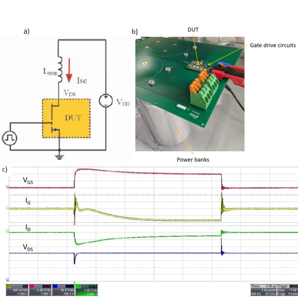
A short circuit test setup allowing to perform type I SC tests was built according to the schematic presented in Fig 1 a). The type I SC test consists of applying a voltage across the power terminals of a device before turning it ON while maintaining the voltage.
The test setup is also presented in Fig 1 b); the setup is composed of a mother-and-daughter board. The motherboard includes the gate drive circuits and the power circuit. While the daughterboard includes the GaN HEMT and some capacitors. The board connection is made with screws for power contacts (Drain and source) and pins for the gate signal.
The data acquisition is made by an oscilloscope. Four signals were recorded during each test; VGS and VDS using passive probes, IG was read with a high-speed differential probe across a 50Ω resistor during OFF-state, and an 8.3Ω during ON-state and ID was read via a coaxial shunt sensor (0.00996Ω).

Fig 1. a) Principle schematic of the Type I short-circuit test setup. b) picture of the test setup. c) typical waveforms
Results and discussion
Before finding safe conditions for SC, a step-stress approach was carried out. At first, a fixed 10µs SC was applied to increase the drain voltage from 200V to failure by a 50V step. Between each step, electrical characterization of the DUT was performed to ensure that it was still functional. After this, steps in terms of duration were performed beginning from 1ms till failure with a 1ms step.
The voltage step stress showed that the critical drain voltage is around 400V, knowing that lower voltages did not have an impact on the component’s electrical characteristics. Regarding the duration step stress, it was found that a failure can happen while applying a 3ms step duration, while lower durations did not affect the part characteristics.
Based on these results, the conditions of the final test were the following:
| Drain voltage | Pulse duration | Number of pulses | |
| Single SC | 200V | 1ms | 1 |
| Repetitive SC | 200V | 500µs | 1000 (10s between each pulse) |
Eight parts were subjected to each SC type. Electrical characteristics were performed before and after the tests. During the test campaign, no critical failure was observed for single nor repetitive SC. The electrical characterization showed that all the parts were still functional, and all the characteristics were inside the datasheet specification. In terms of drifts, only two parts subjected to repetitive short circuits suffered from a significant drift of the gate leakage current, going from the 10µA range before stress to the 100µA range after the stress.
These results indicate that the biggest stressor causing failure for this kind of component in SC conditions is the drain voltage. In fact, when we observe the typical waveforms presented in Fig 1 c), it is clear that the most critical conditions for the DUT are related to the first microseconds of the SC when the current is close to 200A. This huge current rise, coupled with the applied voltage, creates a massive power dissipation in the DUT. When the DUT does not fail during this first step of the test, a decrease in the drain current is observed. This decrease is related to the reduction of the carrier mobility due to the higher junction temperature of the DUT and to the reduction of the VGS, which is related to the increase of the gate leakage current causing a voltage drop across de gate resistor. This drain current reduction also decreases the dissipated power in the DUT, acting as self-protection and increasing the robustness towards SC condition.
GET IN TOUCH TODAY!
Have questions? Contact us
- The behaviour of GaN power HEMTs subjected to short circuit - October 26, 2022

0 comments on The behaviour of GaN power HEMTs subjected to short circuit