SEE testing on GaAs test vehicles. Methodology, Results and Derating.
- Posted by doEEEt Media Group
- On February 19, 2020
- 0
Talk summary:
Radiation sensitivity of GaAs components is not really well known, compare to other technologies. Traditional radiation harness policy consisted in a good derating in DC bias conditions to ensure operation inside a known or expected DC safe operating area (SOA). However destructive single event effects (SEE) have been seen on some MESFET devices under nominal DC bias and RF signal and conditions which were compliant with standard derating requirements.
Many discussion have been arisen during last years regarding necessary SEE radiation testing and derating policy to define a proper SOA: do we need to test or not with RF applied?, what RF signals?, do we need to test other technologies than power MESFET like HEMT, pHEMT?, have we to modify derating rules?.
Under an ESA contract, TAS selected several European technologies (OMMIC D01PH pHEMT; OMMIC ED02AH pHEMT; UMS PPH25X pHEMT; UMS HP07 MESFET) and non-European ones (MITSUBISHI High Power MESFET; Sumitomo “7” Series MESFET, Sumitomo Low Noise pHEMT) to test under DC and DC+RF signals trying to achieve worst case conditions.
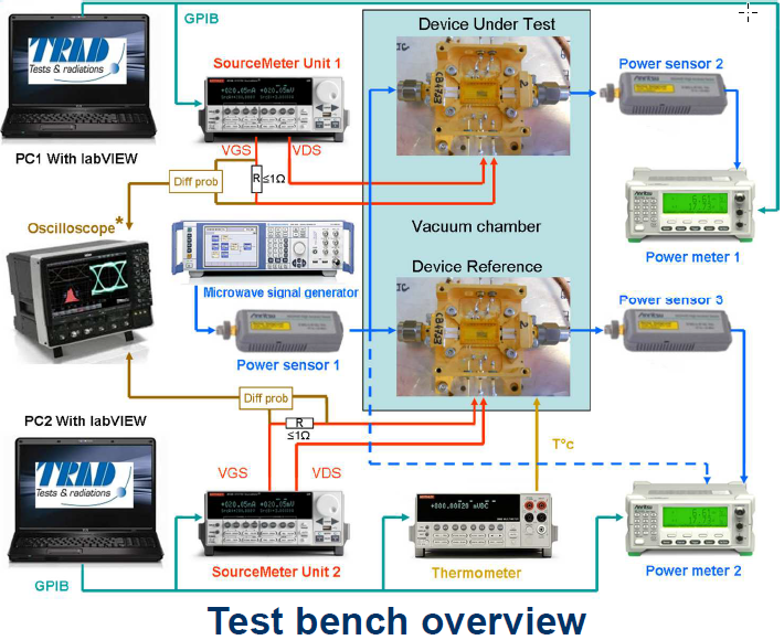
The present paper details test vehicles, test methodology and set-up, test results and derating lessons learned of the SEE heavy ions campaign performed at UCL Belgium test facility last November’2015.
Irradiation Campaign
The irradiation campaign started the perform at the Heavy Ions Cyclotron Facility (HIF) at University of Louvain la Neuve in Belgium, on week 1547 (November 17th to 20th).
Where Ion 124Xenon+35, 995MeV, the Highest LET value available in coctail-2: 62.5 MeV/cm2/mg in Si (effective LET in GaAs of 44.3 MeV/cm2/mg). For other side, the penetration range up to 73.1μm in Si; 49μm in GaAs. Enough for a “sensitive” thickness estimated to be <20μm (including passivation around 1000A SiN, contact metal around 5000A Al, and GaAs uniform doped channel of typical <2000um). The size of the Fluence starting from 106 to 107 ions/cm2 (under orthogonal impact (no tilt). They where practiced from 7 to 12 runs per device. 7 to 10 minutes irradiation per run.
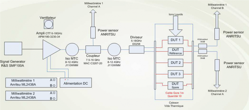
The sample size, on the same board was: 3 DUT for irradiation + 1 REF biased inside the chamber + 1 attrition biased inside the chamber. Also 1 attrition outside the board (chamber). To finish, the Electrical Measurements before and after irradiation was given by two characteristic:
- OUTPUT CHARACTERISTIC : Ids vs (Vds, Vgs)
- SCHOTTKY CHARACTERISTIC : Igs vs Vgs
And took out continuous Monitoring during irradiation: Pin (dBm) & Pout (dBm), Id (A); Ig (A) and Temperature.
Download or read the full report here
- Space-Grade components available for immediate delivery - April 10, 2025
- Managing EEE components for LEO and lower cost space missions - December 17, 2024
- Filtering Characteristics of Parallel-Connected Fixed Capacitors in LCC-HVDC - November 21, 2024


0 comments on SEE testing on GaAs test vehicles. Methodology, Results and Derating.