High Brightness Semiconductor Lasers as Transmitters for Space Lidar Systems
- Posted by Pawel Adamiec
- On February 13, 2020
- 0
Abstract: High brightness semiconductor lasers are potential transmitters for future space lidar systems. In the framework of the European Project BRITESPACE, we propose an all semiconductor laser source for an Integrated Path Differential Absorption lidar system for column-averaged measurements of atmospheric CO2 in future satellite missions. The complete system architecture has to be adapted to the particular emission properties of these devices using a Random Modulated Continuous Wave approach. We present the initial experimental results of the InGaAsP/InP monolithic Master Oscillator Power Amplifiers, providing the ON and OFF wavelengths close to the selected absorption line around 1572 nm.
System Design
Random-Modulation Continuous-Wave Lidar
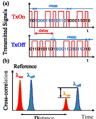
Random-modulation CW (RM-CW) lidar [7] is capable of obtaining range-gated back-scattering information as obtained from pulsed techniques. In RM-CW lidar, a Pseudo-Random Binary Sequence (PRBS) is transmitted (See Fig. 1 (a)). The received signal correlated with the original PRBS code gives a range resolved response with a non-ambiguous range determined by the number of PRBS bits (repetition rate) which can be extended further than the trip time corresponding to the atmosphere thickness. The auto-correlation property of the PRBS and the temporal shifting of the codes can be used to transmit both wavelengths simultaneously, which avoids the beam misalignment problem. Fig. 1 (b) shows an example of the cross-correlation between the received signal and the emitted PRBS. The ratio between the cross-correlation intensities of the reference output and received signals provides information about the differential absorption optical depth and hence on the dry air mixing ratio of CO2. Furthermore, due to the extended non-ambiguity distance, equals to the total PRBS code length, the returns can be binned into different range gates with the distance resolution limited by the PRBS bit time (chip time).
Lidar System
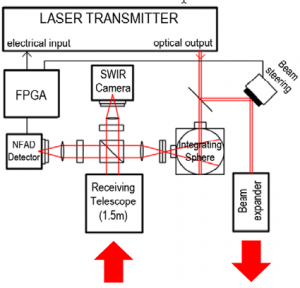
The design of the complete IPDA lidar system is shown in Fig. 2. It consists of the laser transmitter, the optics for beam transmission and reception and the control electronics. Specifically, the output beam from the transmitter is split in two branches: one
is sent to the beam expander and then to the atmosphere and the other is used as reference in the comparison with the received signal, for the calculation of CO2 concentration. The reflected light from Earth ground is collected by a reflective telescope with a Field of View (FOV) matching the laser beam divergence and alignment issues are addressed by using a Short have Infrared (SWIR) camera.
Laser Transmitter
Laser Module
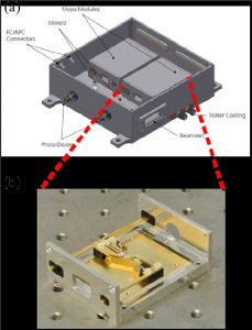
For each laser chip, a sub-module has been designed to provide electrical access, temperature control and beamforming optics for each tapered MOPA. Fig. 4 (a) shows the design of the laser module; Fig. 4 (b) shows a photograph of a real sub-module with a working MOPA without the collimating optics. The radiation emitted by the tapered amplifier is astigmatic, i.e. it has different virtual sources (and different angles of divergence) for the fast axis (vertical direction) and the slow axis (horizontal direction). Due to this characteristic, an optical system for the collimation of a tapered amplifier must consist of two lenses.
Frequency Stabilization Unit
Regarding frequency stability and knowledge accuracy, the most critical is the on-line frequency, due to the slope in the wing of the line.
The linewidth and linewidth knowledge accuracy is expected to be uncritical for the BRITESPACE transmitter, because pseudo-random modulation dominates the linewidth which is therefore well known.
In order to achieve these frequency requirements, we use two opto-electrical feedback loops for the stabilization of the on- and off-channels coupled to the output of a third optoelectrical feedback loop for CO2 locking.
Laser Chip
Three different geometries were initially proposed and fabricated for the laser chip implementation, based on i) straight, ii) tilted, and iii) bended designs. the tilted and bended geometries were proposed in order to minimize undesired optical feedback from the amplifier section to the DFB oscillator. In fact, standard straight monolithically integrated MOPAs exhibit instabilities due to compound cavity effects arising from the residual reflectivity at the amplifier output facet [13, 14]. In order to decrease the reflections at the facets, a simple method consists in tilting the device with regard to the facets. This technique is very common for SOAs. The main drawback is the difficulty to make efficient high reflective coatings on the backside DFB laser facet due to the tilt.
In this paper, we report on the progresses of the BRITESPACE Consortium in order to achieve space-borne lidar measurements of atmospheric carbon dioxide concentration based on an all semiconductor laser source at 1.57 μm.
GET IN TOUCH TODAY!
Do you have questions? Contact us!
Read the full report or downland below
- Image Sensors: Characterization according to the EMVA 1288 standard - February 15, 2022
- Development of a NIR-VIS-UV lidar echo emulator - October 7, 2021
- LIDAR echo emulator - October 7, 2021


0 comments on High Brightness Semiconductor Lasers as Transmitters for Space Lidar Systems