Assessing Radiation Hardness of SIC MOS Structures
- Posted by doEEEt Media Group
- On February 24, 2020
- 0
Motivation and Study Strategy
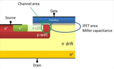
This study aims to support the development of discrete European radiation hardened SiC power MOSFET for use in space applications by means of studying the gate oxide in terms of SEE and TID as one of the key parameters in the future development of these devices. The resistance of the P/N junctions present in these devices was also studied as well taking into account the problems seen in Schottky junctions under heavy ions radiation combined with high voltage.
The following approach to better understand SiC Power MOSFET sensitivity was followed:
- Gate Oxide oxidation process and gate geometry study: 3 oxidation processes + 5 gate geometries tested under gamma and heavy ions
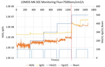
- Heavy Ions test of 600V HV L-DMOS with experimental boron-doped gate oxide that could improve radiation hardness
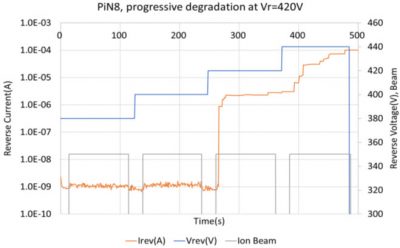
- Heavy ions onto 1200V PIN diodes fully representative of the built-in ones present in power MOSFETs
Gate Oxidation Processes & Geometries
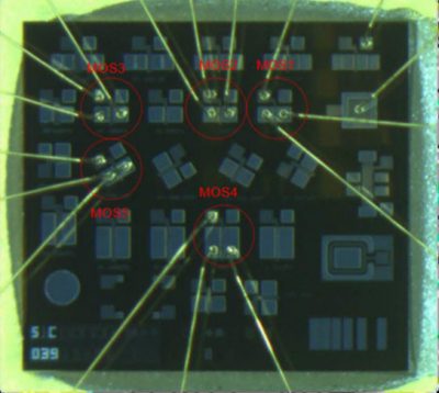
DUTs description: SiC Lateral MOS
- Ox1: Thermally grown gate thin SiO2 oxide in N2O ambient + TEOS deposition 400 Å
- Ox2: Thermally grown gate SiO2 oxide + Boron doped 1 + TEOS 400 Å
- Ox3: Thermally grown gate thin SiO2 oxide in N2O ambient + TEOS deposition 400 Å with oxidation process optimization
Gate Oxidation Results
| wdt_ID | DUT | Gate Width (μm) | Gate Lenght (μm) | Channel Rotation vs Flat |
|---|---|---|---|---|
| 1 | MOS5 | 24 | 150 | 30 |
| 4 | MOS1 | 2 | 150 | 0 |
| 7 | MOS2 | 4 | 150 | 0 |
| 10 | MOS3 | 24 | 150 | 0 |
| 13 | MOS4 | 4 | 300 | 0 |
GET IN TOUCH TODAY!
Do you have questions? Contact us!
Results
| wdt_ID | LET | VGS (V) | VDS (V) | Damage |
|---|---|---|---|---|
| 1 | 10.0 | 0, 2.5, -5 | 0 | no |
| 4 | 20.4 | 0, 2.5, -5 | 0 | no |
| 7 | 32.4 | 0, 2.5, -5 | 0 | no |
| 10 | 10.0 | 0 | up to 500 | no |
| 13 | 20.4 | 0 | up to 500 | PIGS after 400V run |
| 16 | 32.4 | 0 | up to 500 | PIGS after 200V run |
| 19 | 62.5 | 0 | up to 500 | 200V run |
| 22 | 20.4 | -5 | up to 500 | 400V run |
Results:
| wdt_ID | DUT | LET | Vrec Step (V) | Failure at |
|---|---|---|---|---|
| 1 | PiN4 | 62.5 | 100 | degradation @400V |
| 4 | PiN7 | 20.4 | 25 | degradation @400V |
| 7 | PiN1 | 10.0 | 100 | abrupt failure @500V |
| 10 | PiN2 | 20.4 | 100 | abrupt failure @500V |
| 13 | PiN3 | 32.4 | 100 | degradation @400V |
| 16 | PiN8 | 20.4 | 20 | degradation @420V |
| 19 | PiN11 | 32.4 | 20 | degradation @400V |
| 22 | PiN9 | 32.4 | 25 | degradation @400V |
Latest posts by doEEEt Media Group (see all)
- Space-Grade components available for immediate delivery - April 10, 2025
- Managing EEE components for LEO and lower cost space missions - December 17, 2024
- Filtering Characteristics of Parallel-Connected Fixed Capacitors in LCC-HVDC - November 21, 2024

0 comments on Assessing Radiation Hardness of SIC MOS Structures