
Prototyping and Characterization of 1200V Schottky SiC Diode
- Posted by doEEEt Media Group
- On November 25, 2021
- 0
Background
- General requirements of EPC –TWTA
- EPC (Electronic Power Conditioning) for TWT (Travelling Wave Tube) is a converter
- EPC feeds one or two TWT, forming a high-power transmitter.
- provides high voltage up to about 8 kV and average power up to about 300W
- telecommunications satellite can embark from a few tens to over 100 of these sets
- EPC typically operate under a baseplate temperature of about 65°C, while TWT are exposed to baseplate temperatures around 95°C
Allowing the EPC to work at higher temperatures
-
-
- simplification of thermal design,
- a reduction of the distance between the EPC HV section and the TWT
- reduced size and mass
- increased system reliability
-
One of the key element in the high temperature EPC is the diode part of the HV rectifier module
Typical diodes used so far:
- Si diodes in hermetic glass (E.g VMI or Sensitron )
- Problematic supply chain
- Poor performance at high temperature
- Poor switching characteristics
ESA ITT
![]()
- SiC Schottky diode
- Package similar to 6L-LCC that would not require assembly delta validation
- Fully European supply chain
- Capable of continuous operation @ 200°C Tj
- Maintaining some of the key parameters of the Si diode
Introduction
ITT baseline:
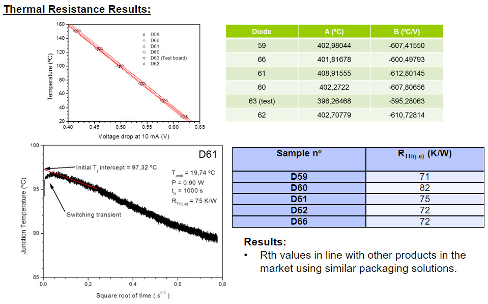
- The study will be focused on the development of high voltage SiC Schottky diode in a package suitable for space application with the primary goal to characterize the performances of the devices in terms of switching capability, reliability of the technology, and preliminary characterization of static and dynamic parameters as a function of temperatures as well as to characterize the thermal impedance and resistance of the proposed package solution.
Requirements
ITT baseline requirements:
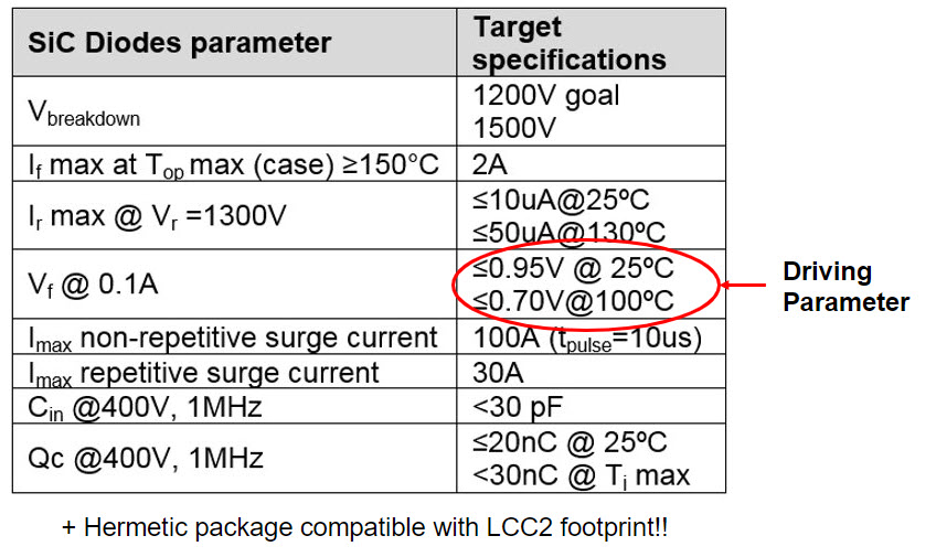 To avoid requalification of potting process -> direct replacement for Si diode currently in use
Review of technical activities
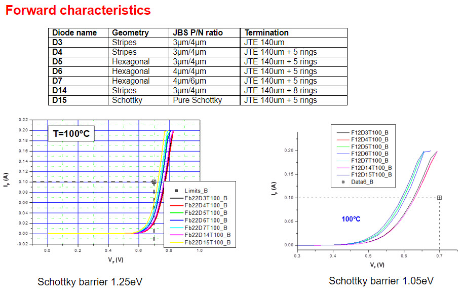
1.Design: JBS design parameters
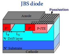
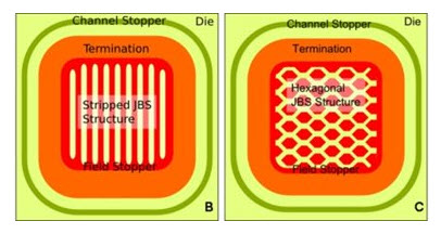
Main JBS design parameters:
- P+ dimensions: Lp and Ln
- P+ mesh geometry: stripes, hexagonal, …
- High voltage termination
- Diode size
2. 1st manufacturing batch
3. Package Design
- Package Specifications
-
- A batch of 205 devices using eutectic Au: Si.
- The leading design rule used for the package design was the form factor required to meet the existing system board device footprint.
- This meant designing a package that was compatible as a drop-in replacement for a D5-B board footprint, similar to a standard 6 Lead Leadless Carrier Chip (6L-LCC) package.
- In order to accommodate the new die design, the standard 6L-LCC package had to be modified with the lead positions kept constant relative to the device centerline.

4. Parts DEscription
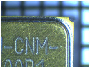
1200V SiC Schottky Diodes: ATN-CNM-1200D1

Main characteristics
- High Voltage Capability (tested up to 1500V)
- Low Vfwd:
- Vfwd~0.7V at 100mA (25degC)
- Vfwd~0.6V at 100mA (100degC)
- Hermetic Package
- LCC2 custom package fully compatible with standard LCC2 footprint
5. Evaluation Test Flow

Review of technical activities 1200V SiC Schottky
1.Results: Initial Characterization
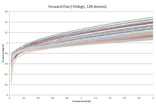
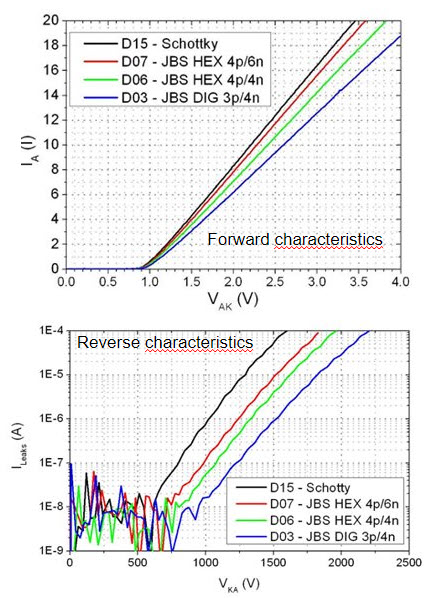
Forward Characterization
- Low Vfwd(@100mA):
- ~0.7V at 25ºC
- ~0.6V at 100ºC
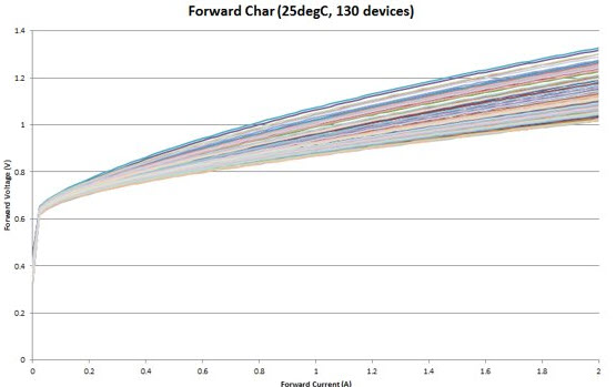

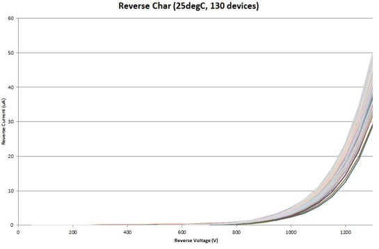
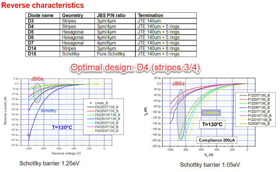
Reverse Characterization (up to 1300V)
- TEC controlled setup for room temp measurements to improve repeatability
- Good stability of the devices while reverse biased
- Low-temperature helpful measurement to screen out devices with latent defects
- Not fully compliant with requirements, high reverse current at high temperature
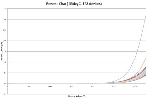
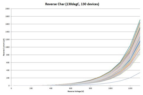
Extended Reverse Characterization
- Devices measured up to 1500V obtained repetitive results.

Schottky Barrier Drift
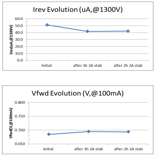
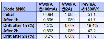
High enough Ifwd applied continuously causes permanent drift of the Schottky Barrier causing:
- Reduction in about 20% of Irev (@1300V)
- Increase in about 1% of Vfwd (@100mA)
Stabilization time:
- Not all the devices stabilize in the same time
- Larger stabilization times needed during screening to ensure a final stable product
Review of technical activities
1. Results: Initial Characterization (Switching)

Destructive and Reliability tests
- Temperature Step Stress
- Power Step Stress
- Maximum Current Test
- Power Cycle Test
- Package Tests
- ESDS Characterization
- Constructional analysis
- HTRB
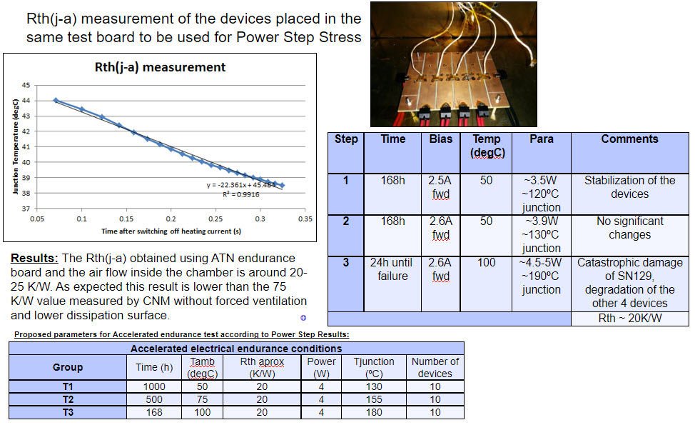
- Accelerated Electrical Endurance
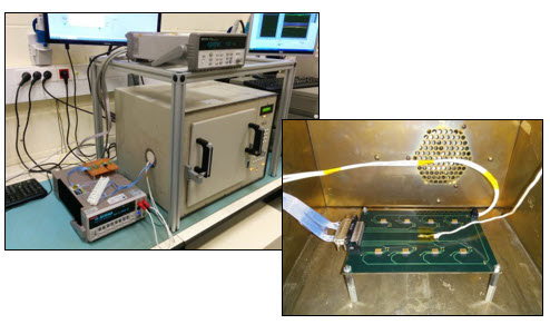
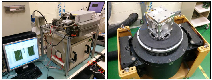
2. Results: Temperature Step Stress
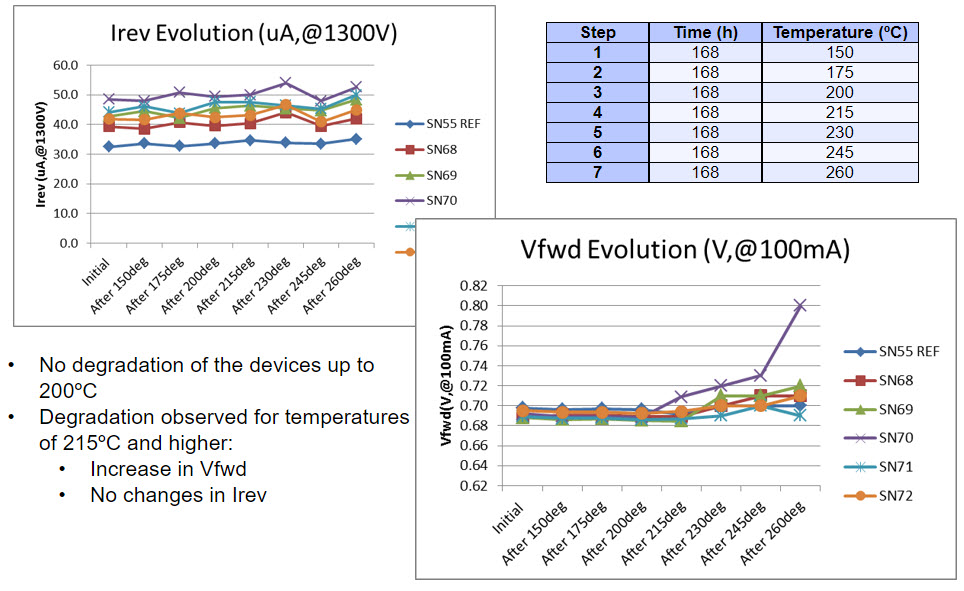
Review of technical activities
3. Results: Maximum Current Tests – Switching Characterization
Destructive Test – Repetitive Peak Forward Current test (IFRM)

Destructive Test – Non-Repetitive Forward Surge Current test (IFSM)

Review of technical activities
3. Results: Power Cycle Test
An active Power Cycling of constant timing (ton=const. andtoff=const.) consistent in a load current conducted through the SiC diode, which is heated by its internal losses generating a temperature gradient in him. When the desired junction temperature is reached, the load current is switched off. The DUT is placed on a heat sink, without forced cooling, and a natural conducted and radiation-cooling phase concludes the cycle.
Power Cycle Test conditions:
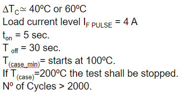
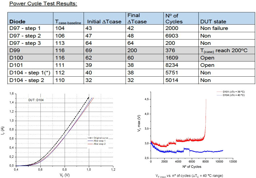
EOL criteria: A 20% increase in the junction temperature swing DTj or a 5% increase in the forward voltage in the SiC diode was defined as failure criteria.
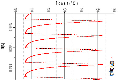
SiC diodes developed can withstand more than 2000 cycles if the case temperature swing is more minor than 40ºC, whit a slight increase (less than 5%) in the forward voltage at 0.1A.
4. Results: Package Tests (Vibration)
SRS Shocks and Sine Vibration
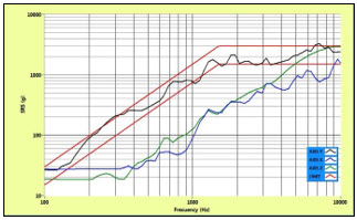
SRS Shocks 1500g, 0.5ms duration, five shocks per axis, Axis Y1, X1, Z1
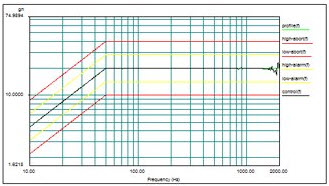
Sine Vibration
Frequency sweep: 10-2000Hz (up and down)
Acceleration: 20g (cross over at 50Hz)
12 sweeps (4 tests in each one of the three axis)
4 minutes each sweep
Intermediate measurement of the devices: No drift
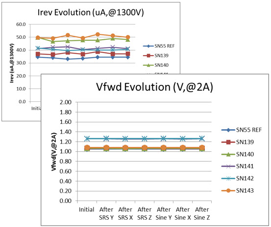
Also Intermediate check of:
Hermeticity (gross and fine leaks) -> OK
Pin to case isolation (1300V) -> OK
5. Results: Package Tests (Thermal Cycling)
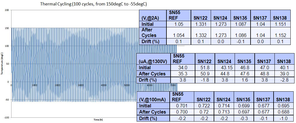
Package Thermal Cycles:
Electrical Characterization before and after the thermal cycles:
6. Results: Constructional Analysis
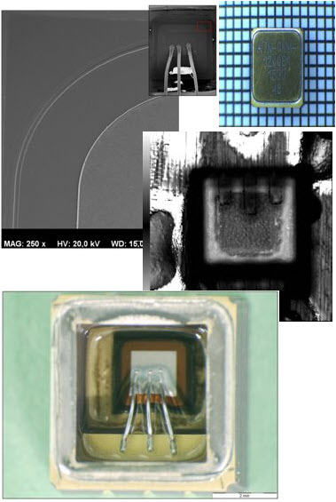
- CSAM -> Good attach of the die in both batches. Lot B exhibits better attachment in the periphery of the die than lot A.
- RGA -> Results consistent with the gel-filled package. No anomalies were observed.
- DPA :
- External Visual Inspection -> No anomalies were observed
- Internal Visual Inspection -> No abnormalities were observed
- Removal of isolating gel -> No damages introduced by gel removal
- SEM Inspection -> No abnormalities were observed
- Bond Pull Test -> 78.95gf mean value, minimum measured was 62.42 (pass criterion: 20gf)
- Die Shear Test -> All the dies withstood more than 10kgf (pass criterion: 2.5kgf)
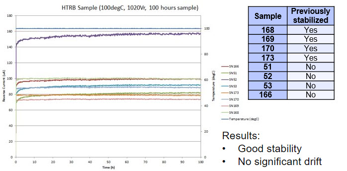
7. Results: Tests HTRB
- Samples: Performed onto both stabilized and non-stabilized devices.
- Duration: 1080 hours
- Ambient Temperature: 100ºC
- Reverse bias 1020 (85% of 1200V)
- Constant monitoring of the reverse currents

8. Results: Accelerated Electrical Endurance

Heavy Ions on SiC Schottky Diodes
Heavy Ions Radiation Test on SiC Schottky Diodes:
- Performed at UCL Cyclotron

Phase 1: Threshold Allocation
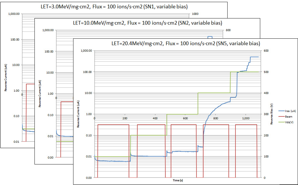
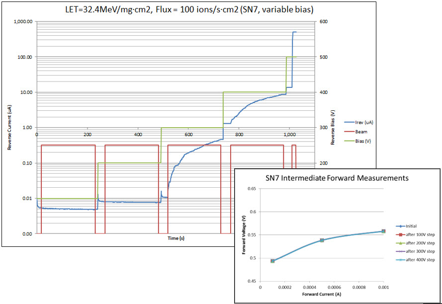
Phase 2: Degradation Evaluation

Safe Operating Area

Critical analysis and next steps
The test campaign evidence:
In the diode design, we have prioritized the forward characteristics;
- All the diodes fully comply with the bold specifications, with a pretty significant margin;
- The ideal case would be to have a Schottky metal with a slightly higher barrier height. Up to now, we did not found a corresponding metal.
- The reverse leakage current is higher than specifications; again, a Schottky metal with a slightly higher barrier would help to approach the specs data.
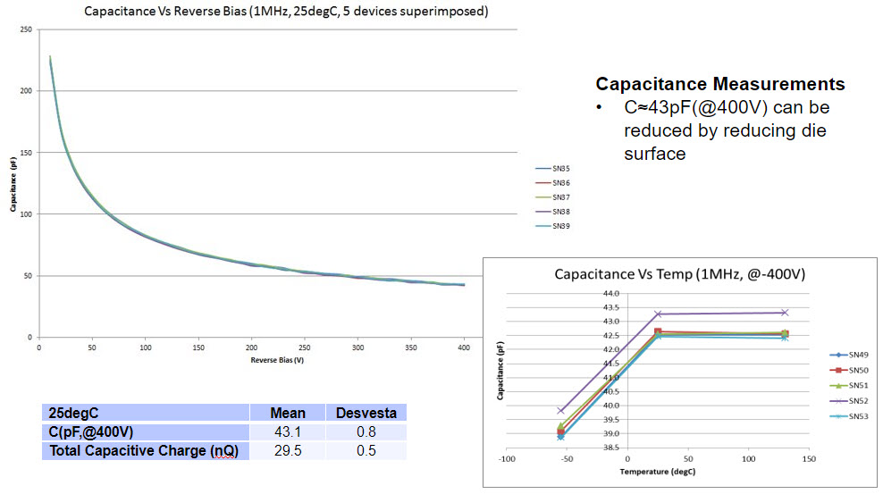
- We could consider a slight reduction of the diode area to better adjust the forward voltage drop to the 0.7V@0.1A@100ºC specified. We could gain on the input capacitance value to reach specs. However, the corresponding reverse current gain would not allow acquiring the specifications.
- The maximum operating temperature is 200ºC and is limited by the package
- There are heavy ions issues
- The joint effort of ATN and CNM in wide SiC devices continues:
- As a continuation of this project, radiation hardening improvements are being implemented by CNM/ATN. Additional heavy ions radiation test campaigns are currently ongoing to validate the behavior of new generations of SiC Schottky diodes

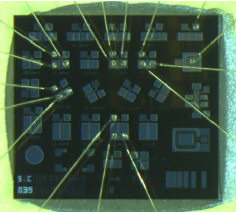
PROTOTYPING AND CHARACTERISATION OF RADIATION-HARDENED SIC MOS STRUCTURES (I)
- Understand the full failure mechanism of SiC technologies regarding manufacturing processes
- Consolidate best design and manufacturing approach for future parts development
Key elements
- Full characterization of several foundries as well as oxidation processes, packaging approaches, etc…
- To consolidate test methods and associated standards for SiC characterization
Other ATN activities regarding SiC devices
Characterization of SiC JFET & MOSFET (II)
- Key Testing parameters:
- Temperature characterization: SiC -> T>150ºC
- High Voltage (up to 1700V) plus high-temperature testing (175ºC)
- High Power Tests: 17A Devices
- Evaluation of maturity of technology for space application:
- Reliability issues of some JFET commercial devices (early stages of normally OFF technology)
- Threshold instabilities in SiC MOSFET
- Good performance of JFET Normally ON products. Life tests with good results.

SiC Schottky Blocking Diode for BepiColombo and Solar Orbiter
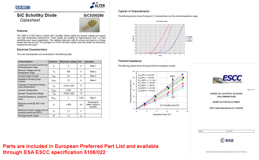
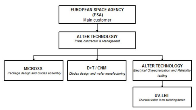
Thanks to ESA, D+T Microelectrónica A.I.E, Universitat de Valencia and Micross components
- Space-Grade components available for immediate delivery - April 10, 2025
- Managing EEE components for LEO and lower cost space missions - December 17, 2024
- Filtering Characteristics of Parallel-Connected Fixed Capacitors in LCC-HVDC - November 21, 2024


0 comments on Prototyping and Characterization of 1200V Schottky SiC Diode