Radiation Sensitive Technologies and EEE Parts
- Posted by Juanjo Medina
- On September 28, 2020
- 0
The object of this post is to define which EEE components and technologies are radiation sensitive. There must be taken into consideration the high relevance in space projects that parts election has. Some radiation effects can be mission limiting where they lead to a prompt or accumulated degradation which results in subsystem or system failure, or catastrophic system anomalies. Other effects can be a source of interference, degrading the efficiency of the mission.
There must be considered radiation effects on the matter is a huge field of knowledge. The main goal of this post is to clearly summarize in a schematic way which EEE parts/technologies are sensitive to each different radiation effect.
For a better understanding, the information is split into 3 points that represent the different radiation mechanisms which affect an electronic component, giving a brief introduction of each as well as presenting a summary table of technologies and effects.
Total Ionizing Dose Effects
It is a cumulative long-term ionizing damage. Ionization induced in semiconductor materials or associated insulators, such as silicon dioxide layers, can lead to charge trapping or the formation of interface states at the semiconductor‐insulator boundary, affecting component behaviour or material properties. In MOS devices, the trapped charge can lead to a shift in the gate threshold voltage, and for semiconductors in general, interface states can significantly increase device leakage currents. Materials such as polymers and glasses are also susceptible to total ionizing dose (TID) effects and can suffer degradation in mechanical, electrical and optical properties.
The atomic particles involved in TID effects are electrons, protons and bremsstrahlung.
Table 1 identifies the technologies used in space applications whose TID effects shall be analyzed.
Table 1. Technologies sensitive to Total Ionizing Dose effects
Displacement Damage Effects
Displacement damage (also referred to as non‐ionizing dose damage) is a cumulative damage process induced by energetic particles and which affect components such as optoelectronics, bipolar devices, and solar cells. The damage mechanism is because of collisions with atoms to displace them from lattice positions creating interstitials and vacancies. These interstitials and vacancies are mobile and can cluster together or react with impurities in the lattice structure creating stable defect centres. The overall effect of displacement damage (DD) is a change in the minority carrier lifetimes of semiconductors and increased light absorption and colouration in crystalline optical materials.
The atomic particles that contribute DD effects are protons, electrons, neutrons and ions.
Table 2 shows below DD sensitive technologies and their effects.
Table 2. Technologies sensitive to Displacement Damage effects
Single Event Effects
Single event effects are a collection of phenomena whereby microelectronics can be disrupted or permanently damaged by single incident particles (as opposed to effects like total ionizing dose where cumulative damage occurs from many particles). Protons and heavier ions, and neutrons can induce such effects. In the case of heavy ions, this occurs by direct ionization of sensitive regions of the semiconductor, and for protons and neutrons, their nuclear interactions within or very near to the active semiconductor can produce localized charge generation.
SEE phenomena can be divided into two sub‐groups:
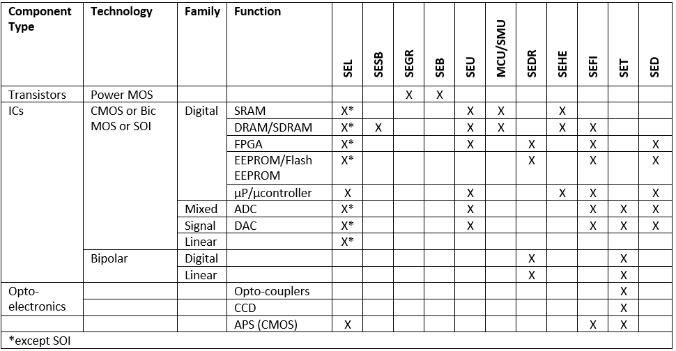
- Destructive effects, where high‐current conditions are induced which have the potential to destroy the device. SEE examples include single event latch‐up (SEL), single event gate rupture (SEGR), single event burn‐out (SEB), and single event snap‐back (SESB)
- Non‐destructive effects, in which data are corrupted or the device is placed in a different operational state or power cycling is employed to return the state of the device to its normal condition. Examples of such effects include single event upset (SEU), multiple‐bit upset (MBU), multiple‐cell upset (MCU), single‐word multiple‐bit upsets (SMU), single event functional interrupt (SEFI), single event hard error (SEHE), single event disturb (SED), and single event transient (SET).
Below, Table 3 showing technologies and components susceptible to SEE effects. If one of those is intended to be used in a space mission, SEE probability and effects shall be assessed.
Tables 1, 2 and 3 are taken from ECSS–ST-10-12C standard of the European Cooperation for Space Standardization.
Future posts will develop certain aspects such as deep analysis of each radiation mechanism, components validation testing, radiation design margins or shielding solutions for space used parts.
- Radiation Sensitive Technologies and EEE Parts - September 28, 2020
- Declared Component List. EEE Components for Space. - May 7, 2020
- Parts Approval Document (PAD). EEE components testing. - May 7, 2020


0 comments on Radiation Sensitive Technologies and EEE Parts