Passive Components in 3D Packaging: The View from ECTC
- Posted by doEEEt Media Group
- On June 27, 2019
- 0
Of the 40 or so technical sessions, several were notable in that they focused on research involving the embedding and integration of passive components in 3D configurations. Here are some examples.
Thin-Film Capacitors
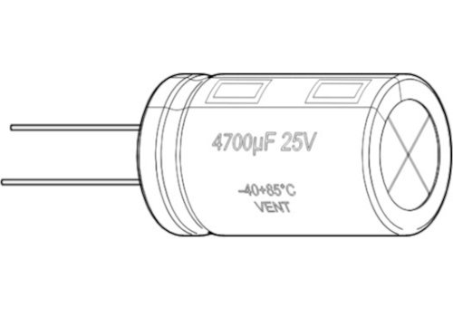
Embedding thin-film capacitors (TFCs) in a package substrate aims to improve the performance of a power supply. Tomoyuki Akahoshi, Daisuke Mizutani, et al. of Fujitsu reported on three structures for package substrates with embedded TFCs that promise to dramatically reduce the impedance on power supply lines and provide a stable power supply to the IC.
In their paper “Improved Structure for Package Substrates with Embedded Thin-Film Capacitor,” the authors note that as the voltages of ICs have been reduced in recent years, restricting the ripple voltage during IC operations has become an issue as designers seek to improve the performance of electronic devices.
Placing a decoupling capacitor near the IC chip is an effective way of restricting the voltage fluctuation, and this has been achieved by placing capacitors on the surface and bottom side of the package substrate. However, this approach has a drawback in that the power supply impedance is not reduced at high frequencies due to the effects of power line resistance and inductance.
The authors propose three structures for package substrates with embedded TFCs – namely, single-sided embedded TFC structures, standalone embedded TFC structures, and coreless embedded TFC structures.
By combining the proposed structures, the authors note that it is possible to place the required capacitance in the relevant locations, and placing the inductors in the empty locations facilitates the manufacture of RC or LC circuits.
The researchers claim this technology can be applied not only to Flip Chip BGA (FCBGA) package substrates for high-end CPUs, but also to optical-module substrates that require high-density components and power-supply design constraints, as well as DC-DC converters that control the voltages of nearby devices.
The main challenges for RF modules intended for consumer products, which integrate switches, a low noise amplifier, and a power amplifier, are small size, small thickness, low cost, good RF performance, and good thermal performance. The latter two challenges are largely dependent on packaging technology.
On one hand, heatsink very-thin quad-flat no-leads (HVQFN) solutions are known to be effective in terms of thermal properties. High-frequency applications, however, suffer from high insertion losses and poor matching due to wire bonds.
On the other hand, flip-chip based solutions are effective from an RF point of view but have bad thermal properties. Excellent RF grounding is key for the successful implementation of many RF functions, but the best solution in terms of grounding often is a bad one from a thermal point of view.
3D Integrated Passive Devices
In their paper “Ultra-thin QFN-Like 3D Package with 3D Integrated Passive Devices,” Ayad Ghannam of 3DiS Technologies, Niek van Haare of Besi Netherlands, Philippe Meunier of NXP France and Julian Bravin of EV Group E. Thallner GmbH describe a new wafer-level 3D packaging technology developed to enable integration of a QFN-like (quad-flat, no-leads) 3D package targeting both effective electrical and thermal properties and having a thickness of less than 200 μm. The proposed architecture allows 3D interconnection of stacked, staggered dies and integration of 3D integrated passive devices inside the package for added functionality and electrical performance.
The 3D Integrated Passive Devices (IPD) package was developed using laser temporary debonding, accurate pick and place, high-density 3D-RDL (redistribution layer) over vertical sidewalls, and very thin cap transfer-molding.
It’s hard to argue with results: Target total thickness was 200 μm or less for this package (tolerance < ±10%) and a cap thickness smaller than 50 μm was successfully demonstrated. Additionally, high-performance 3D-IPD devices were successfully integrated inside the package and exhibited Q values as high as 51.
This result showed the 3D integration capability of this concept, making it suitable for RF 3D wafer-level system-in-packages. The package concept was used to produce a prototype with an RF device inside, improving electrical performance compared to wire-bond based solutions through short 3D interconnects and improving thermal dissipation compared to flip-chip based solutions by spreading heat through the PCB.
Voltage Regulators
Today’s voltage regulator architectures can create major bottlenecks to power efficiency due to long power delivery networks (PDNs). Current needs to travel a long distance from the voltage regulator (VR) to power the IC chips, resulting in high DC loss and low power efficiency due to Joule heating. As such, PDNs with short interconnection length and low DC resistance are highly desired for voltage regulators.
At ECTC, Teng Sun, Robert G. Spurney et al. of the Georgia Institute of Technology’s 3D Systems Packaging Research Center, along with Furukawa Yoshihiro of Nitto Denko Corp., presented a paper entitled “3D Packaging with Embedded High-Power-Density Passives for Integrated Voltage Regulators.” They reported on 3D integration of inductors and capacitors embedded into substrates and placed close to the chips in voltage regulators for high-power applications such as AI computing and servers, resulting in short power delivery networks (PNDs) and high power efficiency.
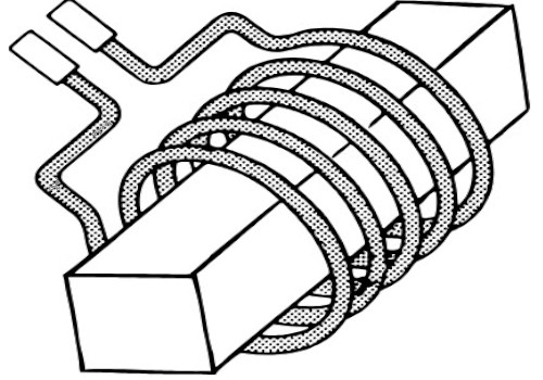
High-density tantalum capacitors were integrated with high-density magnetic-core inductors to create voltage regulators with module thickness around 0.7 mm. The tantalum capacitors featured a capacitance density of ~1 μF/mm2 at a thickness of only 100 μm.
By incorporating high-permeability magnetic materials as the cores, the inductors achieved 20X improvement in inductance compared to air-core inductors. The high inductance allowed inductors to be designed with fewer windings, resulting in low component resistance. When the 3D LC networks are used in high-power applications, the low DC resistance mitigates joule heating and thermal stress problems in the LC networks.
With this 3D integration approach, the LC networks are placed close to the AI chips to reduce interconnection length and improve power efficiency.
Integrated Capacitors
The constant demand for miniaturization, added functionality and increased performance in electronic devices is driving a growing interest in component and system integration technologies – especially in the form of 3D and 2.5D packaging technologies with integrated capacitors.
In order to avoid consuming precious space on the chip surface, clever methods need to be implemented to increase the surface area of the electrode without increasing the footprint area of the device. One flexible and suitable option is to use an on-chip, fully solid-state device based on carbon nanofibers.
To that end, A. M. Saleem, R. Andersson, et al., of Smoltek AB presented a paper titled “Fully Solid-State Integrated Capacitors Based on Carbon Nanofibers and with Specific Capacitances higher than 200 nF/mm2”. The capacitors under study use vertically aligned carbon nanofibers (VACNFs) as electrodes to provide a large 3D surface in a metal-insulator-metal (MIM) configuration. They were manufactured and characterized in terms of capacitance per device footprint area, equivalent series resistance (ESR), breakdown voltage and leakage current.
The researchers realized a capacitance density on the order of 200 nF/mm2 from devices with a 250nm pitch and 15nm of HfO2 as a dielectric material. A high capacitance value of 152 nF was obtained from a single device with a footprint area of 0.7056 mm2, which is 14 times higher than that of a parallel plate device with the same configuration.
Ti/Cu was found to be the best metal combination for the bottom electrodes of the capacitors, and by de-embedding, the ESR of the devices was found to be about 100 ohms with an overall profile height of fewer than 4 microns and breakdown voltages of up to 25 V.
The process was reported to be completely CMOS compatible. This, along with the low device profile, makes these devices readily available for integration on a CMOS chip, in 3D stacking or on redistribution layers in a 2.5D interposer technology.
Source: TTI Market Eye article
by Murray Slovick. The Electronic Components and Technology Conference (ECTC), sponsored by the IEEE Electronics Packaging Society, brought together engineering talent in packaging and components for four days of technical exchange at the Cosmopolitan of Las Vegas, May 28-31.
- Managing EEE components for LEO and lower cost space missions - December 17, 2024
- Filtering Characteristics of Parallel-Connected Fixed Capacitors in LCC-HVDC - November 21, 2024
- ALTER SPACE TEST CENTER: testing approaches for New Space - September 30, 2024


0 comments on Passive Components in 3D Packaging: The View from ECTC